
SEMICONDUCTOR DEVICE PHYSICS AND DESIGN
5.3.1 Schottky Barrier Height .....219 5.3.2 Capacitance Voltage Characteristics .....223 5.3.3 Current Flow across a Schottky Barrier: Thermionic Emission .....223 5.3.4 Comparison of Schottky and p-ndiodes . .....227 5.4 METAL SEMICONDUCTOR JUNCTIONS ...
Download SEMICONDUCTOR DEVICE PHYSICS AND DESIGN

Information
Domain:
Source:
Link to this page:
Related documents
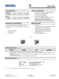
B320 - B360
www.diodes.com3.0A SURFACE MOUNT SCHOTTKY BARRIER RECTIFIER Keywords: This Schottky Barrier Rectifier has been designed to meet the general requirements of commercial applications. It is ideally suited for use as: · Polarity Protection Diode · Re-Circulating Diode · Switching Diode Created Date: 2/17/2016 10:00:29 AM
Chapter 1 Power Electronic Devices (Part I)
pdfs.semanticscholar.orgSchottky diode (Schottky barrier diode-SBD) standard recovery Reverse recovery time and charge specified. t rr is usually less than 1μs, for many less than 100 ns —— ultra-fast recovery diode. – A majority carrier device – Essentially no recovered charge, and lower forward voltage. – Restricted to low voltage (less than 200V)

BAT54SLT1 - Dual Series Schottky Barrier Diodes
www.onsemi.comThese Schottky barrier diodes are designed for high speed switching applications, circuit protection, and voltage clamping. Extremely low forward voltage reduces conduction loss. Miniature surface mount package is excellent for hand held and portable applications where space is limited.

Edition 3.0 2016-04 INTERNATIONAL STANDARD NORME ...
webstore.iec.cha) Schottky barrier diodes and its properties are added; b) Clauses 3, 4 , 5 and 7 were amended with some deletions of information no longer in use or already included in other parts of the IEC 60747 series, and some necessary with