Transcription of Class A Amplifier Design - Learn About Electronics
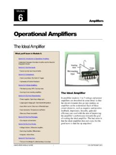
1 AC THEORY MODULE 1 E. COATES 2007 -2012 Class A Amplifier Design Introduction to Amplifier Design Basic Design process. Fig. shows a Class A common emitter Amplifier , but without its component values. This module shows how to simply calculate the values needed to make a working Amplifier that has correct Class A bias as described in Amplifier Module and so produce an undistorted and amplified output. Building and testing an Amplifier is a good way Learn how and why an Amplifier works. How will you know that your calculations are correct? The best way is to build your Design and test it. Follow the guidelines in this section and download the accompanying pdf documents, so you can Design , build and test a working Amplifier . Although Amplifier Design can be a complex process, this simple exercise takes some short cuts, because it is more concerned with learning About how an Amplifier works, rather than designing a complete new hi-fi system.
2 Amplifiers Module 2 What you ll Learn in Module 2. Section Introduction to Amplifier Design . Section DC Conditions. Design a BJT Class A common emitter audio Amplifier . Section AC Conditions. Calculate suitable values for AC components. build a prototype Amplifier on Breadboard. Section Testing the Amplifier . Test the Amplifier for Gain, Bandwidth, Input and Output Impedance. Section Improving the Amplifier . Carry out tests and modifications, and apply Negative Feedback to achieve specified performance criteria. Section Multi-stage Amplifiers. Describe methods for inter-stage coupling in multi-stage amplifiers: Section Amplifier Design Quiz. Test your knowledge & understanding of basic Amplifier Design . Fig. Common Emitter Amplifier Class A Amplifier Design AMPLIFIERS MODULE 2 E.
3 COATES 2007 - 2012 Amplifier Design Project Sections to of this module are a practical project to Design a single stage Class A common emitter Amplifier . Use information from other sections modules in learnabout- Electronics (just click the links where needed) to help you calculate the component values needed for a working Amplifier . The only maths involved will be some Ohms law and some capacitive reactance calculations. The Amplifier Design Record Download and print out the Amplifier Design Record, which can be used in conjunction with sections to of this module so you will have a complete record of how to Design , build and test an Amplifier . It contains all the formulae needed to calculate the correct DC and AC conditions for the Amplifier , and once the Amplifier Design is complete, the prototype circuit can be easily built on breadboard (Proto board). The project also shows you how to test an Amplifier for performance using a multi meter and oscilloscope.
4 The project is split into four sections so that it can be checked for errors as the Design progresses. By splitting the Design task in this way, there is far less chance of going wrong. Carefully follow the Design sequence instructions on line in sections to of this module, and record the results of your calculations and tests on the Amplifier Design Record sheets to Design and build a working Class A common emitter Amplifier . This is a great way to understanding how an Amplifier works. Class A Amplifier Design AMPLIFIERS MODULE 3 E. COATES 2007 - 2012 Module Class A Amplifier Design Part 1. Designing the DC Conditions. Calculate the component values and record your results in Part 1 of the Amplifier Design Record sheets.
5 1. Decide on the DC supply voltage VCC This should be less than the maximum VCEO voltage for the transistor you intend to use and will also depend on the available supply; this may be a bench power supply or a battery. Values of 6 to 12 volts are common for a common emitter voltage Amplifier . 2. Choose a transistor The prototype Amplifier for this exercise used a NPN small signal transistor such as the 2N3904, but other similar transistors should work equally well. A datasheet for the 2N3904 can be downloaded from or you could choose a different general purpose NPN small signal transistor and download its datasheet. 3. Decide on a suitable quiescent collector current Iq Iq is the Collector current when no signal is applied. The maximum value must be less than the maximum VCEO figure for the transistor. However using a high value of current will waste power as the circuit is supposed to be a VOLTAGE Amplifier so current should be kept quite low, but the lower the current you choose, the higher the value of RL will be.
6 This increases the output impedance of the Amplifier (which will be approximately the value of the load resistor) and ideally this should be low. A compromise figure of around 10 to 20% of the transistor s IcMAX figure shown on the data sheet should be adequate for Iq and a commonly selected current of around 1mA would be typical. What you ll Learn in Module After studying this section, you should be able to: Design a basic Class a Common emitter audio Amplifier . Understand appropriate Design and component requirements for a Class A Amplifier . Calculate resistance values for DC bias conditions. Assemble a prototype Amplifier on Breadboard. Use a multimeter to carry out appropriate tests to confirm operation. Fig. Amplifier DC components As you work through the Design process, record your results of your calculations and Design decisions on the Amplifier Design Record sheets that you can also download from by clicking any of the links to Amplifier Design Record sheets.
7 You will need these results when building the Amplifier . Class A Amplifier Design AMPLIFIERS MODULE 4 E. COATES 2007 - 2012 4. Calculating a value for the load resistor RL Once the supply voltage and collector current are decided, the value of the collector resistor can be calculated. The transistor quiescent collector voltage needs to be About half of VCC so that the output signal can swing by equal amounts above and below this value without driving the transistor into saturation (0V and maximum collector current) or cut off (zero current and VC equal to the supply voltage). RL will therefore be half of VCC divided by Iq. Note that whenever a component value has been calculated, it is unlikely that the result of the calculation will match any of the available preferred values of real resistors.
8 Therefore you will need to choose the nearest preferred value. 5. Calculating the value of RE To provide efficient bias stabilisation, the emitter voltage VE should be About 10% to 15% of VCC. So choosing a value of 12% of VCC for VE and assuming that IE is the same as IC (It is only different by the small amount of the base current), a value for the resistor RE can be calculated by dividing the emitter voltage VE by the emitter current IE then choosing the nearest preferred value. 6. Estimate a value for base current IB This can be found by dividing the collector current IC by the transistor s current gain hfe obtained from the data sheet. Because the hfe varies from one transistor to another, even of the same type, it may be quoted as a typical value or as a range between minimum and maximum values, hfe also varies with collector current so whatever figure you choose for hfe, the result of calculating IB will be an approximation so the base voltage will probably not be accurate.
9 However this can be fine tuned when the Amplifier is being constructed. 7. Calculating VB The base voltage should be About (700mV) higher than VE to ensure that the input signal is biased on the linear part of the transistor input characteristic. 8. Calculating the DC bias network current. To ensure adequate bias stability, the current flowing through R1 and R2 should be About 10 times greater than the base current IB so the current flowing through R1 and R2 will be simply IB x 10. 9. Calculating the resistance for R1 The value of this resistor will be the difference between VCC and VB divided by the bias network current through R1 and R2. 10. Calculating the resistance for R2 The value of R2 will be the base voltage VB divided by the bias network current through R1 and R2. Class A Amplifier Design AMPLIFIERS MODULE 5 E.
10 COATES 2007 - 2012 11. Start constructing the Amplifier Fit the transistor and the four resistors in place on the breadboard together with any necessary wire links (Do NOT fit any capacitors yet). Then after a thorough visual check that everything is correctly connected, connect the power supply, switch on and use a multimeter to check the voltages on collector, base and emitter of the transistor. If the voltages are correct you have successfully designed the DC conditions. If there are any drastically wrong voltages, ( more than 30% high or low) check that all the connections on the Amplifier are correct, and that you have read the resistor colour codes correctly. Any smaller differences may need the value of one or more of the resistors changing. Try to make collector voltage VC exactly half of the supply voltage VCC. If it already is, well done! If not (which is most likely) the first thing to check is that you have correctly calculated the values of RL and RE and fitted the nearest preferred value of resistor in both positions.