Transcription of 500mA Low-Noise LDO Voltage Regulator
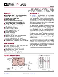
1 SPX3819 500mA Low-Noise LDO Voltage Regulator July 2018 Rev. 1/13 Rev. GENERAL DESCRIPTION The SPX3819 is a positive Voltage Regulator with a low dropout Voltage and low noise output. In addition, this device offers a very low ground current of 800 A at 100mA output. The SPX3819 has an initial tolerance of less than 1% max and a logic compatible ON/OFF switched input. When disabled, power consumption drops to nearly zero. Other key features include reverse battery protection, current limit, and thermal shutdown. The SPX3819 includes a reference bypass pin for optimal low noise output performance. With its very low output temperature coefficient, this device also makes a superior low power Voltage reference. The SPX3819 is an excellent choice for use in battery-powered applications such as cordless telephones, radio control systems, and portable computers.
2 It is available in several fixed output Voltage options or with an adjustable output Voltage . This device is offered in 8 pin NSOIC, 8 pin DFN and 5-pin SOT-23 packages. APPLICATIONS Portable Consumer Equipment Portable Instrumentation Industrial Equipment SMPS Post regulators FEATURES Low noise : 40 V Possible High Accuracy: 1% Reverse Battery Protection Low Dropout: 340mV at Full Load Low Quiescent Current: 90 A Zero Off-Mode Current Fixed & Adjustable Output Voltages: , , , , , & Fixed Output Voltages Adjustable Output Voltages Available in RoHS Compliant, Lead Free Packages: 5-pin SOT-23, 8-pin SOIC and 8-pin DFN TYPICAL APPLICATION DIAGRAM Fig. 1: SPX3819 Application Circuit SPX3819 500mA Low-Noise LDO Voltage Regulator 2/13 Rev. ABSOLUTE MAXIMUM RATINGS These are stress ratings only and functional operation of the device at these ratings or any other above those indicated in the operation sections of the specifications below is not implied.
3 Exposure to absolute maximum rating conditions for extended periods of time may affect reliability. VIN, EN .. -20V to +20V Storage Temperature .. -65 C to 150 C Junction Temperature .. 150 C Power Dissipation .. Internally Limited Lead Temperature (Soldering, 5 sec) .. 260 C ESD Rating (HBM - Human Body Model) .. 1kV OPERATING RATINGS Input Voltage Range VIN .. to 16V Enable Pin EN .. to VIN Junction Temperature Range .. -40 C to +125 C Thermal Resistance1 .. JA (SOT23-5) ..191 C/W JA (NSOIC-8) .. C/W JA (DFN-8) .. 59 C/W Note 1: The maximum allowable power dissipation is a function of maximum operating junction temperature, TJ(max) the junction to ambient thermal resistance, and the ambient JA, and the ambient temperature TA. The maximum allowable power dissipation at any ambient temperature is given: PD(max) = (TJ(max)-TA)/ JA, exceeding the maximum allowable power limit will result in excessive die temperature; thus, the Regulator will go into thermal shutdown.
4 ELECTRICAL SPECIFICATIONS Specifications with standard type are for an Operating Junction Temperature of TJ = 25 C only; limits applying over the full Operating Junction Temperature range are denoted by a . Minimum and Maximum limits are guaranteed through test, design, or statistical correlation. Typical values represent the most likely parametric norm at TJ = 25 C, and are provided for reference purposes only. Unless otherwise indicated, VIN = VOUT + 1V (VIN = VOUT + for option), IL = 100 A, CL = 1 F, VEN , TA= TJ = 25 C. Parameter Min. Typ. Max. Units Conditions Output Voltage Tolerance -1 +1 % -2 +2 Output Voltage Temperature Coefficient 57 ppm/ C Line Regulation %/V VIN = VOUT +1 to 16V and VEN 6V VIN = VEN = VOUT +1 8V VIN = VEN = VOUT +1 16V TA = 25 C to 85 C Load Regulation % IL = to 500mA Dropout Voltage (VIN-VOUT) 2 10 60 mV IL = 100 A 80 125 175 IL = 50mA 250 180 350 IL = 150mA 450 340 550 IL = 500mA 700 Quiescent Current (IGND) 3 A VENABLE 8 VENABLE = Ground Pin Current (IGND) 90 150 A IL = 100 A 190 250 650 IL = 50mA 900 mA IL = 150mA IL = 500mA Ripple Rejection (PSRR) 70 dB SPX3819 500mA Low-Noise LDO Voltage Regulator 3/13 Rev.
5 Current Limit (ILIMIT) 800 mA VOUT=0V Current Limit (ILIMIT) Output noise (eNO) 950 mA VRMS VOUT=0V IL = 10mA, CL = F, CIN = 1 F, (10Hz 100kHz) 300 Output noise (eNO) Input Voltage Level Logic Low (VIL) 40 VRMS IL = 10mA, CL = F, CBYP = 1 F, CIN = 1 F, (10Hz 100kHz) V OFF Input Voltage Level Logic High (VIH) 2 V ON ENABLE Input Current 2 A VIL VIH ENABLE Input Current 3 20 A VIL VIH Note 2: Not applicable to output Voltage 2V or less. PIN ASSIGNMENT Fig. 2: SPX3819 Pin Assignment PIN DESCRIPTION Name Pin # nSOIC Pin # DFN Pin # SOT-23 Description VIN 2 3 1 Supply Input GND 5, 6, 7, 8 7 2 Ground VOUT 3 5 5 Regulator Output EN 1 1 3 Enable(input). CMOS compatible control input. Logic high enable; logic low or open = shutdown ADJ 4 8 4 Adjustable part only. Feedback input. Connect to resistive Voltage -divider network BYP Fixed version only.
6 Internal reference bypass pin. Connect 10nF to ground to reduce thermal noise on the output. NC - 2, 4, 6 - No Connect SPX3819 500mA Low-Noise LDO Voltage Regulator 4/13 Rev. ORDERING INFORMATION(1) Part Number Operating Temperature Range Lead-Free Package Packaging Method SPX3819M5-L/TR -40 C TJ +125 C Yes(2) SOT-23-5 Tape & Reel SPX3819M5-L-1-2/TR SPX3819M5-L-1-5/TR SPX3819M5-L-1-8/TR SPX3819M5-L-2-5/TR SPX3819M5-L-3-0/TR SPX3819M5-L-3-3/TR SPX3819M5-L-5-0/TR SPX3819R2-L/TR DFN-8 SPX3819R2-L-1-2/TR SPX3819S-L/TR NSOIC-8 SPX3819S-L-5-0/TR NOTES: 1. Refer to for most up-to-date Ordering Information 2. Visit for additional information on Environmental Rating. SPX3819 500mA Low-Noise LDO Voltage Regulator 5/13 Rev. TYPICAL PERFORMANCE CHARACTERISTICS Fig. 3: Ground Current vs Load Current Fig. 4: Ground Current vs Input Voltage Fig. 5 Ground Current vs Load Current in Dropout Fig.
7 6 Output Voltage vs Input Voltage Fig. 7 Dropout Voltage vs Load Current Fig. 8 Output Voltage vs Load Current SPX3819 500mA Low-Noise LDO Voltage Regulator 6/13 Rev. Fig. 9 Ground Current vs Temperature with 100 A Load Fig. 10 Ground Current vs Temperature with 50mA Load Fig. 11 Ground Current vs Temperature with 500mA Load Fig. 12 Ground Current vs Temperature in Dropout Fig. 13 ENABLE Voltage , ON threshold, vs Input Voltage Fig. 14 Output Voltage vs Temperature SPX3819 500mA Low-Noise LDO Voltage Regulator 7/13 Rev. Fig. 15 Output noise vs Bypass Capacitor Value IL = 10mA, 10Hz - 100kHz Fig. 16 Line Transient Response for Device Fig. 17 Load Transient Response for Device APPLICATION INFORMATION The SPX3819 requires an output capacitor for device stability. Its value depends upon the application circuit. In general, linear Regulator stability decreases with higher output currents.
8 In applications where the SPX3819 is sourcing less current, a lower output capacitance may be sufficient. For example, a Regulator outputting only 10mA, requires approximately half the capacitance as the same Regulator sourcing 150mA. Bench testing is the best method for determining the proper type and value of the capacitor since the high frequency characteristics of electrolytic capacitors vary widely, depending on type and manufacturer. A high quality F aluminum electrolytic capacitor works in most application circuits, but the same stability often can be obtained with a 1 F tantalum electrolytic. With the SPX3819 adjustable version, the minimum value of output capacitance is a function of the output Voltage . The value decreases with higher output voltages, since closed loop gain is increased.
9 TYPICAL APPLICATIONS CIRCUITS For fixed Voltage options only. A 10nF capacitor on the BYP pin will significantly reduce output noise , but it may be left unconnected if the output noise is not a major concern. The SPX3819 start-up speed is inversely proportional to the size of the BYP capacitor. SPX3819 500mA Low-Noise LDO Voltage Regulator 8/13 Rev. Applications requiring a slow rampup of the output Voltage should use a larger CBYP. However, if a rapid turn-on is necessary, the BYP capacitor can be omitted. The SPX3819 s internal reference is available through the BYP pin. Figure 18 represents a SPX3819 standard application circuit. The EN (enable) pin is pulled high (> ) to enable the Regulator . To disable the Regulator , EN < Fig. 18: Standard Application Circuit The SPX3819 in Figure 19 illustrates a typical adjustable output Voltage configuration.
10 Two resistors (R1 and R2) set the output Voltage . The output Voltage is calculated using the formula: VOUT = x [1 + R1/R2] R2 must be >10k and for best results, R2 should be between 22k and 47k . Fig. 19: Typical Adjustable Output Voltage Configuration SPX3819 500mA Low-Noise LDO Voltage Regulator 9/13 Rev. MECHANICAL DIMENSIONS 8-PIN SOICN SPX3819 500mA Low-Noise LDO Voltage Regulator 10/13 Rev. MECHANICAL DIMENSIONS (CONTINUED) 8-PIN 2X3 DFN SPX3819 500mA Low-Noise LDO Voltage Regulator 11/13 Rev. RECOMMENDED LAND PATTERN AND STENCIL 8-PIN 2X3 DFN SPX3819 500mA Low-Noise LDO Voltage Regulator 12/13 Rev. MECHANICAL DIMENSIONS (CONTINUED) 5-PIN SOT-23 SPX3819 500mA Low-Noise LDO Voltage Regulator 13/13 Rev. REVISION HISTORY Revision Date Description 08/23/12 Reformat of Datasheet Addition of SPX3819R2-L and SPX3819R2-L/TR part numbers 12/02/13 Added Storage Temperature Range and Junction Temperature in ABS MAX Ratings.