Transcription of Optocoupler, Phototransistor Output, with Base …
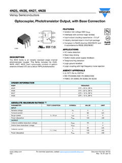
1 Document Number: 81181 For technical questions, contact: , 07-Jan-10153 optocoupler , Phototransistor output , with base Connection4N35, 4N36, 4N37 vishay Semiconductors DESCRIPTIONEach optocoupler consists of gallium arsenide infrared LEDand a silicon NPN APPROVALS Underwriters laboratory file no. E52744 BSI: EN 60065:2002, EN 60950:2000 FIMKO; EN 60065, EN 60335, EN 60950 certificate no. 25156 FEATURES Isolation test voltage 5000 VRMS Interfaces with common logic families Input- output coupling capacitance < pF Industry standard dual-in-line 6 pin package Compliant to RoHS directive 2002/95/EC and inaccordance to WEEE 2002/96/ECAPPLICATIONS AC mains detection Reed relay driving Switch mode power supply feedback Telephone ring detection Logic ground isolation Logic coupling with high frequency noise rejectioni179004-5123654 BCEACNC21842 ORDER INFORMATIONPARTREMARKS4N35 CTR > 100 %, DIP-64N36 CTR > 100 %, DIP-64N37 CTR > 100 %, DIP-6 ABSOLUTE MAXIMUM RATINGS (1)
2 PARAMETERTEST CONDITIONSYMBOLVALUEUNITINPUTR everse voltageVR6 VForward currentIF50mASurge currentt 10 sIFSM1 APower dissipationPdiss70mWOUTPUTC ollector emitter breakdown voltageVCEO70 VEmitter base breakdown voltageVEBO7 VCollector currentIC50mAt 1 msIC100mAPower dissipationPdiss70mWCOUPLERI solation test voltageVISO5000 VRMSC reepage 7mmClearance 7mmIsolation thickness between emitter and detector technical questions, contact: Number: 81181154 Rev. , 07-Jan-104N35, 4N36, 4N37 vishay SemiconductorsOptocoupler, Phototransistor output , with base Connection Notes(1)Tamb = 25 C, unless otherwise in excess of the absolute maximum ratings can cause permanent damage to the device.
3 Functional operation of the device is notimplied at these or any other conditions in excess of those given in the operational sections of this document. Exposure to absolutemaximum ratings for extended periods of the time can adversely affect reliability.(2)Refer to wave profile for soldering condditions for through hole devices (DIP).Notes(1)Tamb = 25 C, unless otherwise and maximum values are testing requirements. Typical values are characteristics of the device and are the result of engineeringevaluation. Typical values are for information only and are not part of the testing requirements.(2)Indicates JEDEC registered tracking indexDIN IEC 112/VDE 0303, part 1175 Isolation resistanceVIO = 500 V, Tamb = 25 CRIO1012 VIO = 500 V, Tamb = 100 CRIO1011 Storage temperatureTstg- 55 to + 150 COperating temperatureTamb- 55 to + 100 CJunction temperatureTj100 CSoldering temperature (2) s dip soldering.
4 Distance to seating plane mmTsld260 CELECTRICAL CHARACTERISTICS (1)PARAMETERTEST capacitanceVR = 0 V, f = 1 MHzCj50pFForward voltage (2)IF = 10 = 10 mA, Tamb = - 55 current (2)VR = 6 ACapacitanceVR = 0 V, f = 1 MHzCO25pFOUTPUTC ollector emitter breakdownvoltage(2)IC = 1 mA4N35 BVCEO30V4N36 BVCEO30V4N37 BVCEO30 VEmitter collector breakdownvoltage(2)IE = 100 ABVECO7 VOUTPUTC ollector base breakdownvoltage (2)IC = 100 A, IB = 1 A4N35 BVCBO70V4N36 BVCBO70V4N37 BVCBO70 VCollector emitter leakage current (2)VCE = 10 V, IF = 04N35 ICEO550nA4N36 ICEO550nAVCE = 10 V, IF = 04N37 ICEO550nAVCE = 30 V, IF = 0,Tamb = 100 C4N35 ICEO500 A4N36 ICEO500 A4N37 ICEO500 ACollector emitter capacitanceVCE = 0 CCE6pFCOUPLERR esistance, input output (2)VIO = 500 VRIO1011 Capacitance, input outputf = 1 MAXIMUM RATINGS (1)PARAMETERTEST CONDITIONSYMBOLVALUEUNIT Document Number: 81181 For technical questions, contact: , 07-Jan-101554N35, 4N36, 4N37 optocoupler , Phototransistor output , with base ConnectionVishay Semiconductors Note(1)Indicates JEDEC registered (1)Indicates JEDEC registered CHARACTERISTICSTamb = 25 C, unless otherwise speciedFig.
5 1 - Forward Voltage vs. Forward Current Fig. 2 - Normalized Non-Saturated and Saturated CTR Current Fig. 3 - Normalized Non-Saturated and Saturated CTR Current Fig. 4 - Normalized Non-Saturated and Saturated CTR CurrentCURRENT TRANSFER RATIOPARAMETERTEST current transfer ratio (1)VCE = 10 V, IF = 10 mA4N35 CTRDC100%4N36 CTRDC100%4N37 CTRDC100%VCE = 10 V, IF = 10 mA,TA = - 55 C to + 100 C4N35 CTRDC4050%4N36 CTRDC4050%4N37 CTRDC4050%SWITCHING CHARACTERISTICSPARAMETERTEST time (1)VCC = 10 V, IC = 2 mA, RL = 100 ton, toff10 - Forward Current (mA)VF -Forward Voltage (V)TA = - 55 CTA = 25 CTA = 85 - LED Current (mA)NCTRNCTR(SAT)NCTR - Normalized CTRCTRCE(sat) = VVCE = 10 V, IF = 10 mA, TA = 25 CTA = 25 CNormalized - LED Current (mA)NCTR - Normalized CTRCTRCE(sat) VCE = VNCTRNCTR(SAT)
6 TA = 50 CNormalized to:VCE = 10 V, IF = 10 mA, TA = 25 - LED Current (mA)NCTR - Normalized CTRNCTRNCTR(SAT)TA = 70 CNormalized to:CTRCE(sat) VCE = VVCE = 10 V, IF = 10 mA, TA = 25 C technical questions, contact: Number: 81181156 Rev. , 07-Jan-104N35, 4N36, 4N37 vishay SemiconductorsOptocoupler, Phototransistor output , with base Connection Fig. 5 - Normalized Non-Saturated and Saturated CTR Current Fig. 6 - Collector Emitter Current and LED Current Fig. 7 - Collector Emitter Leakage Current vs. Temperature Fig. 8 - Normalized CTRcb vs. LED Current and Temperature Fig. 9 - Normalized Photocurrent vs. IF and Temperature Fig. 10 - Normalized Non-Saturated hFE Current and - LED Current (mA)NCTR - Normalized CTRNCTRNCTR(SAT)TA = 85 CNormalized to:CTRCE(sat) VCE = VVCE = 10 V, IF = 10 mA, TA = 25 Ci4n25_0660504030201000510152025303550 C70 C85 CIF - LED Current (mA)ICE - Collector Current (mA)25 Ci4n25_07100806040200- 2010- 210- 1100101102103104105 Tamb- Ambient Temperature ( C)ICEO - Collector Emitter (nA)TypicalVCE = 10 C50 C70 CIF - LED Current (mA) NCTRcb - Normalized to:VCB = V, IF = 10 mA, TA = 25 - LED Current (mA)Normalized = 10 mA, TA = 25 CNib, TA = - 20 CNormalized to.
7 Nib, TA = 20 CNib, TA = 50 CNib, TA = 70 - base Current ( A)1101001000IB = 20 A, VCE = 10 V,TA = 25 C25 C70 C- 20 CNhFE - Normalized to: Document Number: 81181 For technical questions, contact: , 07-Jan-101574N35, 4N36, 4N37 optocoupler , Phototransistor output , with base ConnectionVishay Semiconductors Fig. 11 - Normalized hFE vs. base Current and Temperature Fig. 12 - Propagation Delay vs. Collector Load Resistor Fig. 13 - Switching Timing Fig. 14 - Switching C- 20 C50 C70 CNhFE(sat) - Normalized Saturated hFE1101001000 VCE = 10 V, Ib = 20 ATA = 25 CVCE = VIb - base Current ( A)Normalized to:i4n25_121101001000RL - Collector Load Resistor (k )tPLH- Propagation Delay ( s) = 10 mA, TA = 25 CVCC = V, Vth = VtPLHtPHLtPHL - Propagation Delay ( s)i4n25_13 IFtR= VVOtDtStFtPHLtPLHVTHi4n25_14 VCC = 5 Vf = 10 kHzDF = 50 %RLVOIF = 10 mA technical questions, contact: Number: 81181158 Rev.
8 , 07-Jan-104N35, 4N36, 4N37 vishay SemiconductorsOptocoupler, Phototransistor output , with base Connection PACKAGE DIMENSIONS in millimetersPACKAGE 2 36 5 to YWW 24 Legal Disclaimer Revision: 08-Feb-171 Document Number: 91000 Disclaimer ALL PRODUCT, PRODUCT SPECIFICATIONS AND DATA ARE SUBJECT TO CHANGE WITHOUT NOTICE TO IMPROVE RELIABILITY, FUNCTION OR DESIGN OR OTHERWISE. vishay Intertechnology, Inc., its affiliates, agents, and employees, and all persons acting on its or their behalf (collectively, vishay ), disclaim any and all liability for any errors, inaccuracies or incompleteness contained in any datasheet or in any other disclosure relating to any makes no warranty, representation or guarantee regarding the suitability of the products for any particular purpose or the continuing production of any product.
9 To the maximum extent permitted by applicable law, vishay disclaims (i) any and all liability arising out of the application or use of any product, (ii) any and all liability, including without limitation special, consequential or incidental damages, and (iii) any and all implied warranties, including warranties of fitness for particular purpose, non-infringement and merchantability. Statements regarding the suitability of products for certain types of applications are based on vishay s knowledge of typical requirements that are often placed on vishay products in generic applications.
10 Such statements are not binding statements about the suitability of products for a particular application. It is the customer s responsibility to validate that a particular product with the properties described in the product specification is suitable for use in a particular application. Parameters provided in datasheets and / or specifications may vary in different applications and performance may vary over time. All operating parameters, including typical parameters, must be validated for each customer application by the customer s technical experts. Product specifications do not expand or otherwise modify vishay s terms and conditions of purchase, including but not limited to the warranty expressed as expressly indicated in writing, vishay products are not designed for use in medical, life-saving, or life-sustaining applications or for any other application in which the failure of the vishay product could result in personal injury or death.