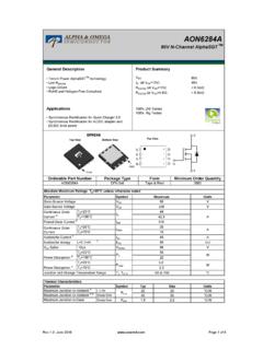
Transcription of P-Channel 60-V (D-S) 175 °C MOSFET
1 vishay SiliconixSUM110P06-08 LDocument Number: 73045S-80273-Rev. B, 60-V (D-S) 175 C MOSFETFEATURES TrenchFET Power MOSFET Package with Low Thermal Resistance 100 % Rg TestedPRODUCT SUMMARY VDS (V)rDS(on) ( )ID (A)d- at VGS = - 10 V - at VGS = - V TO-263 SDGTop ViewOrdering Information:SUM110P06-08 LSUM110P06-08L-E3 (Lead (Pb)-free)SGDP- channel MOSFETN otes: a. Duty cycle 1 %.b. When Mounted on 1" square PCB (FR-4 material).c. See SOA curve for voltage Limited by Package.* Pb containing terminations are not RoHS compliant, exemptions may MAXIMUM RATINGS TC = 25 C, unless otherwise notedParameter Symbol LimitUnit Drain-Source Voltage VDS- 60 VGate-Source Voltage VGS 20 Continuous Drain Currentd(TJ = 175 C)
2 TC = 25 CID- 110 ATC = 125 C- 75 Pulsed Drain CurrentIDM- 200 Avalanche CurrentL = mHIAS- 85 Single Pulse Avalanche EnergydEAS211mJMaximum Power DissipationTC = 25 CPD272cWTA = 25 Junction and Storage Temperature Range TJ, Tstg- 55 to 175 CTHERMAL RESISTANCE RATINGSP arameter Symbol LimitUnit Junction-to-Ambient PCB MountdRthJA40 * Number: 73045S-80273-Rev. B, 11-Feb-08 vishay SiliconixSUM110P06-08 LNotes:a.
3 Pulse test; pulse width 300 s, duty cycle 2 %.b. Guaranteed by design, not subject to production testing. c. Independent of operating temperature. Stresses beyond those listed under Absolute Maximum Ratings may cause permanent damage to the device. These are stress ratings only, and functional operationof the device at these or any other conditions beyond those indicated in the operational sections of the specifications is not implied. Exposure to absolute maximumrating conditions for extended periods may affect device TJ = 25 C, unless otherwise notedParameter Symbol Test Conditions StaticDrain-Source Breakdown VoltageV(BR)DSSVGS = 0 V, ID = - 250 A - 60 VGate-Threshold VoltageVGS(th)
4 VDS = VGS, ID = - 250 A - 1- 3 Gate-Body LeakageIGSSVDS = 0 V, VGS = 20 V 100nAZero Gate Voltage Drain CurrentIDSSVDS = - 60 V, VGS = 0 V - 1 AVDS = - 60 V, VGS = 0 V, TJ = 125 C - 50 VDS = - 60 V, VGS = 0 V, TJ = 175 C - 250On-State Drain CurrentaID(on) VDS = - 5 V, VGS = - 10 V - 120 ADrain-Source On-State ResistancearDS(on) VGS = - 10 V, ID = - 30 A VGS = - 10 V, ID = - 30 A, TJ = 125 = - 10 V, ID = - 30 A, TJ = 175 = - V, ID = - 20 Transconductanceagfs VDS = - 15 V, ID = - 50 A 20 SDynamicbInput CapacitanceCissVGS = 0 V, VDS = - 25 V, f = 1 MHz 9200pFOutput CapacitanceCoss975 Reverse Transfer CapacitanceCrss 760 Total Gate ChargecQgVDS = - 30 V, VGS = - 10 V, ID = - 110 A 160240nCGate-Source ChargecQgs 40 Gate-Drain ChargecQgd 36 Gate ResistanceRgf = 1 Tu r n - O n D e l a y T i m ectd(on)
5 VDD = - 30 V, RL = ID - 110 A, VGEN = - 10 V, RG = 2030nsRise Timectr190285 Turn-Off Delay Timectd(off) 140210 Fall Timectf300450 Source-Drain Diode Ratings and Characteristics TC = 25 CbContinuous CurrentIS- 110 APulsed CurrentISM- 200 Forward VoltageaVSDIF = - 50 A, VGS = 0 V- Recovery TimetrrIF = - 50 A, di/dt = 100 A/ s 6090nsPeak Reverse Recovery ChargeIRM(REC)- 3- Recovery CDocument Number: 73045S-80273-Rev. B, SiliconixSUM110P06-08 LTYPICAL CHARACTERISTICS 25 C, unless otherwise notedOutput CharacteristicsTransconductanceCapacitan ce040801201602000246810 VDS Drain-to-Source Voltage (V) Drain Current (A)IDVGS = 10 thru 5 V3 V4 V040801201602000 1020304050607080ID Drain Current (A) Transconductance (S)gfsTC = - 55 C25 C125 C030006000900012000150000 102030405060 VDS Drain-to-Source Voltage (V)C Capacitance (pF)CissCossCrssTransfer CharacteristicsOn-Resistance vs.
6 Drain CurrentGate Charge040801201602000123456 VGS Gate-to-Source Voltage (V) Drain Current (A)ID25 C-55 CTC = 125 On-Resistance ( )ID Drain Current (A)rDS(on)VGS = 10 VVGS = V04812162004080120160200240280320 Gate-to-Source Voltage (V)Qg Total Gate Charge (nC)VGSVDS = 30 VID = 110 Number: 73045S-80273-Rev. B, 11-Feb-08 vishay SiliconixSUM110P06-08 LTYPICAL CHARACTERISTICS 25 C, unless otherwise notedOn-Resistance vs. Junction TemperatureAvalanche Current vs. 50 - 250255075100 125 150 175TJ Junction Temperature ( C)VGS= 10 VID = 30 ArDS(on) On-Resistance(Normalized)tin (s) (A) (A) at TA= 25 CIAV (A) at TA= 150 Diode Forward VoltageDrain Source Breakdown Source-to-Drain Voltage (V) Source Current (A)IS100101TJ= 25 CTJ= 150 C566064687276- 50 - 250255075100 125 150 175TJ Junction Temperature ( C)(V)V(BR)DSSID = 250 A Document Number: 73045S-80273-Rev.
7 B, SiliconixSUM110P06-08 LTHERMAL RATINGS vishay Siliconix maintains worldwide manufacturing capability. Products may be manufactured at one of several qualified locations. Reliability data for SiliconTechnology and Package Reliability represent a composite of all qualified locations. For related documents such as package/tape drawings, part marking, andreliability data, see Avalanche and Drain Current vs. Case Temperature05010015020002550751001251501 75TC Case Temperature ( C) Drain Current (A)IDPackage LimitedSafe Operating by rDS(on)* Drain Current (A)ID10 s100 sTC = 25 CSingle Pulse100 ms, DC10 ms1001 msVDS Drain-to-Source Voltage (V)* VGS minimum VGS at which rDS(on)is specifiedNormalized Thermal Transient Impedance, Junction-to-CaseSquare Wave Pulse Duration (s) Effective TransientThermal PulseDuty Cycle = Duty Cycle, D =2.
8 Per Unit Base = RthJA = C/W3. TJM TA = PDMZthJA(t)t1t2t1t2 Notes:4. Surface MountedPDM Document Number: : 18-Jul-081 DisclaimerLegal Disclaimer NoticeVishayAll product specifications and data are subject to change without notice. vishay Intertechnology, Inc., its affiliates, agents, and employees, and all persons acting on its or their behalf(collectively, vishay ), disclaim any and all liability for any errors, inaccuracies or incompleteness contained hereinor in any other disclosure relating to any product. vishay disclaims any and all liability arising out of the use or application of any product described herein or of anyinformation provided herein to the maximum extent permitted by law.
9 The product specifications do not expand orotherwise modify vishay s terms and conditions of purchase, including but not limited to the warranty expressedtherein, which apply to these products. No license, express or implied, by estoppel or otherwise, to any intellectual property rights is granted by thisdocument or by any conduct of vishay . The products shown herein are not designed for use in medical, life-saving, or life-sustaining applications unlessotherwise expressly indicated. Customers using or selling vishay products not expressly indicated for use in suchapplications do so entirely at their own risk and agree to fully indemnify vishay for any damages arising or resultingfrom such use or sale.
10 Please contact authorized vishay personnel to obtain written terms and conditions regardingproducts designed for such applications. Product names and markings noted herein may be trademarks of their respective owners.