Transcription of 433MHz Wide Band FM radio transceiver - Radiometrix
1 Radiometrix Ltd, BiM2A Data Sheet page 1 Features Data rates up to 64kbps Crystal controlled PLL FM circuitry for both Tx and Rx Receiver Sensitivity: -101dBm for 1ppm BER (64kbps) -104dBm for 1ppm BER (10kbps) Supply: - 16V @ 14mA TX (10mW), 25mA TX (25mW), 11mA Rx Usable range up to 300 metres external, 75 metres in building SAW front end filter and full screening RSSI (standard) or carrier detect option Analogue and digital baseband Low profile with small footprint 33 x 23 x 5mm Conforms to European EN 301 489-3 and ETSI EN 300 220-3 (ERP @ 10mW) Conforms to Australian/New Zealand AS/NZS 4268.
2 2003 (ERP @ 25mW) Instead of the SAW-based technology of the BiM2, the BiM2A and BiM2H use a PLL circuit locked to a crystal for better frequency stability over a wider temperature range (-20C to +70C) and supply range ( 16V), at the expense of slightly slower power-up. The BiM2A is available as standard on frequencies of and The BiM2H can be made available if required in an extra-high-power version (BiM2EH), in the same footprint and pinout but giving 100mW nominal output power at - 16V supply with a current consumption of less than 60mA. Applications PDAs, organisers and laptops Handheld terminals EPOS equipment, barcode scanners, belt clip printers Data loggers Audience response systems In-building environmental monitoring and control Security and fire alarms Restaurant ordering systems Vehicle data up/download Evaluation platforms: UNI-EVAL, NBEK + BiM / SMX carrier BiM2A is a half-duplex crystals controlled PLL wideband FM transceiver operating on European SRD band.
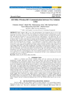
3 It is an enhanced replacement for the SAW based BiM2 and has better frequency accuracy and temperature stability. BiM2H is a high power version with 25mW RF power and specifically made available for Australian/New Zealand users. 433 MHz Wide Band FM radio transceiver433 MHz Wide Band FM radio transceiver433 MHz Wide Band FM radio transceiver433 MHz Wide Band FM radio transceiver Hartcran House, 231 Kenton Lane, Harrow, Middlesex, HA3 8RP, England Tel: +44 (0) 20 8909 9595, Fax: +44 (0) 20 8909 2233, Issue 2, 27 July 2012 BiM2A / BiM2H Fig. 1: BiM2A-433-64 Radiometrix Ltd, BiM2A Data Sheet page 2 Functional overview The transmit section of the BiM2A consists of a frequency modulated crystal locked PLL feeding a buffer amplifier and RF filter.
4 A TX select line controls operation. The transmitter achieves full RF output typically within 1ms of this line being pulled low. Modulation is applied at the TXD input and may be either a serial digital stream toggling between 0V and 3V (digital drive) or a high level analogue waveform with the same peak limits (linear drive). Modulation shaping is performed internally by a 2nd order lowpass filter which minimises spectral spreading. The RF output is filtered to ensure compliance with the appropriate regulations and fed via a Tx/Rx changeover switch to the antenna pin. The receive section is a single conversion FM superhet with an IF of A SAW bandpass filter in the receiver front-end provides image rejection and suppression of other unwanted out-of-band signals.
5 Like the transmitter, the receiver is controlled by its own active low RX select line. A post-detection lowpass filter establishes the signal bandwidth and ensures clean operation of the subsequent adaptive data slicer. The slicer is optimised for balanced data such as bi-phase code. The standard module features a received signal strength (RSSI) output with 60dB of range. A version of BiM2A featuring a fast acting Carrier Detect (CD) output on the same RSSI pin is also available. The CD output will indicate the presence of any RF signals on the carrier frequency. AFRXDM ixerIF bpfdataslicerPA 32 LoopFilterLPF35kHzLPFTXD refosc32 LoopFilterrefosc V C O V C Omatching& lpfpreampTx/Rx switchRegulator& Tx/RxlogicTx selectRx - 16V( - 16V for BiM2EH)Fig.
6 2: Block diagram Pin description RF GND pins 1 & 3 RF ground pins, internally connected to the module screen and to pins 5, 9, 10 & 18 (0V). These pins should be connected directly to the RF return path ( coax braid, main PCB ground plane etc). Antenna pin 2 50 RF connection to the antenna, DC-isolated. See pages 7 & 8 for details of suitable antennas and feeds. 0V (GND) pins 5, 9, 10 & 18 Supply ground connection and screen. RSSI pin 11 Received Signal Strength Indicator with 60dB range, operational when Rx is enabled. Output voltage nominally (no signal), (maximum). See for typical characteristics. CD pin 11 Carrier Detect - When the receiver is enabled, a low indicates a signal above the detection threshold is being received.
7 The output is high impedance (50k ) and should only be used to drive a CMOS logic input. Radiometrix Ltd, BiM2A Data Sheet page 3 RXD pin 12 Digital output from internal data slicer. The output is a squared version of the signal on pin 13 (AF) and may be used to drive a decoder directly. The data is true data, as fed to the transmitter. Output is open-collector format with internal 10k pullup to Vcc (pin 17). AF pin 13 Buffered & filtered analogue output from FM demodulator. Standing DC bias of 1V approx. Useful for test purposes or for driving external decoders.
8 External load should be >10k // <100pF TXD pin 14 This DC-coupled transmitter modulation input will accept either serial digital data or high level linear signals. Drive signal must be limited to 0V min, 3V max (0 - 5V for BiM2EH). See page 5 for suggested drive methods. Input impedance >50k . TX select pin 15 Active-low Transmit select. 47k internal pull-up to Vcc. RX select pin 16 Active-low Receive select. 47k internal pull-up to Vcc. Pin 15 TX Pin 16 RX Function 1 1 Power down (<10 A) 1 0 Receiver enabled 0 1 Transmitter enabled 0 0 Self test loop-back* * Loop-back allows the receiver to monitor the transmitted signal. Under these conditions the Tx radiated signal level will be reduced to approximately -10dBm).
9 Vcc pin 17 DC +ve supply pin. + to +16 volts @ <14mA The supply should be clean, <20mVP-P ripple. 1817161514131211100 VVccRX SELECTTXDTX SELECTAFRXDRSSI/CD0V123456789RF GNDA ntennaRF GND0 VNo pin33 mm23 mm5 mmside view (through can)top view (without can)side view (with can)recommended PCB hole size: mmmodule footprint size: 25 x 32 mmpin pitch: mm ( ")pins 4, 5, 6, 7 are not fitted& 8 Fig. 3: Physical dimensions Weight: 7g (typ.) Radiometrix Ltd, BiM2A Data Sheet page 4 Absolute maximum ratings Exceeding the values below may cause permanent damage to the module. Operating temperature -20 C to +70 C Storage temperature -40 C to +100 C Vcc (pin 17) to +16V TX, RX select (pins 15, 16) -9V to +16V All other pins to +Vcc Antenna (pin 2) 50V DC, +10dBm RF Performance specifications Figures apply to standard version @ Vcc= , temperature +20 C, unless stated.
10 General pin min. typ. max. units notes Supply voltage 17 V Supply voltage (BiM2EH) 17 V Tx supply current @ 10mW 17 - 14 - mA Tx supply current @ 25mW 17 - 25 - mA Tx supply current @ 100mW 17 - 60 - mA Rx supply current 17 10 11 17 mA Note 1 RF centre frequency - - - MHz - Antenna port impedance 2 - 50 - Tx or Rx TX & RX select: high (deselect) 15, 16 Vcc V low (select) 15, 16 0 V Internal select pull-ups 15,16 - 47 - k To Vcc (pin 17) Balanced code bit rate 12 - - 64 kbps -64 version Balanced code bit rate 12 - - 10 kbps -10 version Transmitter section pin min. typ. max. units notes RF power output (BiM2A) 2 +9 +10 +11 dBm RF power output (BiM2H) 2 +13 +14 +15 dBm RF power output (BiM2EH) 3 +19 +20 +21 dBm TX harmonics/spurious emission 2 - -55 -40 dBm Initial centre frequency accuracy - -10 0 +10 kHz FM deviation - 20 27 35 kHz Peak Modulation bandwidth - 0 - 35 kHz @ -3db Modulation distortion - - 5 10 % Note 2 TX spectral bandwidth @-40dBc 2 - - 250 kHz worst case TXD input level: high 14 - V Note 3 high (BiM2EH) 14 - - V Note 3 low 14 0 - V Note 3 TX power up to full RF 2, 15 - 1 ms Note 4 Receiver section pin min.