1d 7
Found 9 free book(s)
MIL-STD-2073 - Standard Practice for Military Packaging
www.woodencrates.orgMIL-STD-2073-1D 15 December 1999 DEPARTMENT OF DEFENSE STANDARD PRACTICE FOR MILITARY PACKAGING AMSC N7296 AREA PACK. MIL-STD-2073-1E ii FOREWORD 1. Details and decision logic for the use of this standard are described in 1.1, 1.2, figure 1, and 6.11. 2. This standard is approved for use by all Departments and Agencies of the Department

1D-The Correction of Common Coding Problems in Urology …
static.aapc.comFerragamo, MA., J. Endourology 17, 7, September 2003 • Procedure: “Ureteroscopic laser lithotripsy of a left ureteral stone and litholapaxy of a bladder stone” – Large (>2.5cm.) bladder stone: 52318-59 594.1 52353-51 592.1 – Small (<2.5cm.) bladder stone 52353 592.1 52317-59-51 594.1 Urology Coding Update
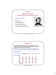
Handout 4 Lattices in 1D, 2D, and 3D - Cornell University
courses.cit.cornell.edu• The volume (3D), area (2D), or length (1D) of a primitive cell can be given in terms of the primitive vectors, and is independent of the choice of the primitive vectors or of the primitive cells a1a2 3 a1. a2 a3 1 a1 1D 2D 3D Example, for the 2D lattice above: 2 …

Mathematics Florida Standards (MAFS) Grade 7
www.fldoe.orgMAFS.7.EE.1.1 Apply properties of operations as strategies to add, subtract, factor, and expand linear expressions with rational coefficients. Cognitive Complexity: Level 1: Recall MAFS. 7.EE.1.2 Understand that rewriting an expression in different forms in a problem context can shed light on the problem and how the quantities in it are related.
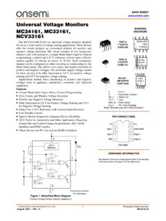
MC34161 - Universal Voltage Monitors - ON Semiconductor
www.onsemi.comVS 7 2 3 + 1.27 V + 1.27 V + 2.8 V + 0.6 V +-8 5 2.54 V Reference-+-+ +-4 This device contains 141 transistors. PDIP−8 P SUFFIX CASE 626 1 SOIC−8 D SUFFIX CASE 751 1 MARKING DIAGRAMS x = 3 or 4 A = Assembly Location WL, L = Wafer Lot YY, Y = Year WW, W = Work Week G or = Pb−Free Package PIN CONNECTIONS Vref Input 1 Input 2 GND VCC Mode ...
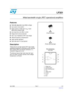
Wide bandwidth single JFET operational amplifiers
www.st.com7 - VCC+ 8 - N.C. Pin connections (top view) www.st.com. Schematics LF351 2/14 1 Schematics Figure 1. Schematic diagram Figure 2. Input offset voltage null circuit Output Non-inverting input Inverting input V CC V CC 100W 1.3k 30k 35k 100W 8.2k Offset Null1 Offset Null2 100W 200W.

AC 91.21-1D - Use of Portable Electronic Devices Aboard ...
www.faa.gov10/27/17 AC 91.21-1D . receivers since they were determined to interfere with the operation of aircraft navigation and communication systems. The FAA subsequently determined other PEDs could be ... paragraph 7.2 (below) of this AC, or equivalent methods specifically accepted by the FAA. If the operator lacks the personal knowledge of these ...
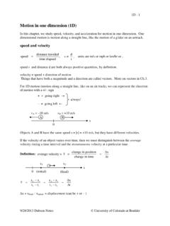
Motion in 1D - Physics
physicscourses.colorado.edu1D - 7 9/28/2013 Dubson Notes University of Colorado at Boulder The direction of the acceleration For 1D motion, the acceleration, like the velocity, has a sign ( + or – ). Just as with velocity, we say that positive acceleration is acceleration to the right, and negative acceleration is …
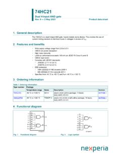
Dual 4-input AND gate - Nexperia
assets.nexperia.comNexperia 74HC21 Dual 4-input AND gate 10. Dynamic characteristics Table 7. Dynamic characteristics GND = 0 V; test circuit see Fig. 8. Symbol Parameter Conditions 25 °C -40 °C to +85 °C -40 °C to +125 °C