Cmos Vlsi Design
Found 11 free book(s)
Introduction to CMOS VLSI Design
www3.nd.edu3 Design Rules CMOS VLSI Design Slide 5 Feature Size Feature size improves 30% every 2 years or so – 1/√2 = 0.7 reduction factor every “generation” – from 1 μm (1000 nm) in 1990 to 14 nm in 2015. – 10 generations in 20 years • 1000, 700, 500, 350, 250, 180, 130, 90, 65, 45, 32, 22, 14, 10 nm 0 10 20 30 40 50 60 70 80 90 2005 2010 2015 2020 2025 2030 ...

High Speed CMOS VLSI Design Lecture 2: Logical Effort & …
pages.hmc.eduNov 04, 1997 · Static CMOS gates are a “ratioless” circuit family, meaning that the gates will work cor-rectly for any ratio of PMOS sizes to NMOS sizes. However, the ratios do influence switching threshold and delay, so it is important to optimize the P/N ratio for high speed designs.
Lecture 19: SRAM
user.engineering.uiowa.edu19: SRAM CMOS VLSI Design 4th Ed. 4 Array Architecture 2n words of 2m bits each If n >> m, fold by 2k into fewer rows of more columns Good regularity – easy to design Very high density if good cells are used

Lecture 7: Power
user.engineering.uiowa.edu7: Power CMOS VLSI Design 4th Ed. 26 Gate Leakage Extremely strong function of t ox and V gs – Negligible for older processes – Approaches subthreshold leakage at 65 nm and below in some processes An order of magnitude less for pMOS than nMOS Control leakage in the process using t ox > 10.5 Å
Chapter 1 Introduction to CMOS Circuit Design
www.ee.ncu.edu.twIntroduction to CMOS Circuit Design Jin-Fu Li Advanced Reliable Systems (ARES) Lab. Department of Electrical Engineering National Central University ... Design Flow for a VLSI Chip Specification Behavioral Design Structural Design Physical …

NOTE: This flow chart is provided as a guide; the catalog ...
www.usf.eduCMOS-VLSI Design Lab 1 hr F COP 2510 Programming Concepts 3 hrs F, S, Su CSE Elective 3 hrs F, S, Su COP 4600 Operating Systems 3 hrs F, S CDA 4213 CMOS-VLSI Design 3 hrs F CIS 4250 Ethical Issues & Prof Conduct (TGEE) 3 hrs F, S CDA 3103 Computer Organization 3 hrs F, S, Su COT 4400 Analysis of Algorithms 3 hrs F, S, Su
CMOS VLSI Design - Pearson
www.pearsonhighered.comCMOS VLSI Design A Circuits and Systems Perspective. Fourth Edition Neil H. E. Weste Macquarie University and The University of Adelaide David Money Harris Harvey Mudd College CMOS VLSI Design A Circuits and Systems Perspective Addison-Wesley Boston Columbus Indianapolis New York San Francisco Upper Saddle River
CMOS Comparator Design
www.eecis.udel.eduPre-amp Design A fully ... “A 1 V 6 b 50 MHz current-interpolating CMOS ADC,” in Symp. VLSI Circuits, 1999, pp. 79-80. M 1 M 2 M 5 M 3 M 4 V i + V i-V o + V o-R L R L X. Vishal Saxena -22- Pre-amp Example

CMOS Technology and Logic Gates - MIT OpenCourseWare
ocw.mit.eduCMOS VLSI is thedigital implementation technology of choice for the foreseeable future (next 10-20 years) – Excellent energy versus delay characteristics – High density of wires and transistors – Monolithic manufacturing of devices and interconnect, cheap! 6.884 – Spring 2005 2/07/2005 L03 – CMOS Technology 4

Combinational Logic Gates in CMOS - Purdue University
engineering.purdue.eduStatic CMOS Circuit • At every point in time (except during the switching transients) each gate output is connected to either V DD or V SS via a low-resistive path • The outputs of the gates assume at all times the value of the Boolean function, implemented by the circuit • In contrast, a dynamic circuit relies on temporary
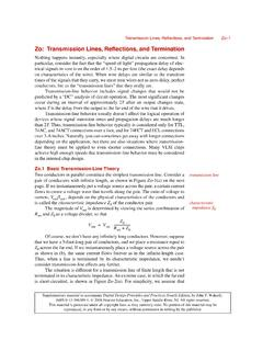
Zo:Transmission Lines, Reflections, and Termination
web.cecs.pdx.eduCMOS driver switches from LOW to HIGH, the 5 V source in the driver sees the 150-Ω resistance of the driver in series with the 150- Ω Z 0 of the line, so a 2.5-V wave propagates down the line. After time T, this wave reaches the receiving gate U2 onthe far end and is reflected.After time 2T, the reflected wave reaches