Current Circuits 12
Found 6 free book(s)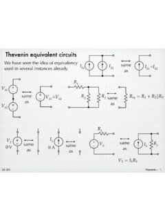
Thevenin equivalent circuits - Iowa State University
tuttle.merc.iastate.eduJun 10, 2014 · Thevenin equivalent circuits ... 12 V 1 k! R L R L R v i P 1 ! 11.99 mV 11.99 mA 0.144 mW ... load resistance, calculate the load voltage (and current and power) for each of the circuits. The results are identical. In terms of the load that is attached at the port, the two circuits are indistinguishable. Check it yourself. EE 201 Thevenin – 5
Chapter 31 Alternating Current Circuits
www.austincc.eduMFMcGraw-PHY 2426 Chap31-AC Circuits-Revised: 6/24/2012 24 Average Power - Inductors Inductors don’t dissipate energy, they store energy. The voltage and the current are out of phase by 90 o. As we saw with Work, energy changed only when a portion of the force was in the direction of the displacement. In electrical circuits energy is
Chapter 8 Natural and Step Responses of RLC Circuits
www.ee.nthu.edu.twCircuits 8.1-2 The Natural Response of a Parallel RLC Circuit. 8.3 The Step Response of a Parallel . RLC . ... The inductor current cannot change abruptly, 6 General solution 0. ... 12.5 kHz, 2(200)(2 10 ) 1 2 1 0 2. 7 7. LC RC ...
EE105 – Fall 2014 Microelectronic Devices and Circuits
inst.eecs.berkeley.eduof interest and provide open circuits at dc. • C 1 and C 2 are low impedance coupling capacitors or dc blocking capacitors whose reactance at the signal frequency is designed to be negligible. • C 3 is a bypass capacitor that provides a low impedance path for ac current from emitter to ground, thereby removing R E (required for

Noise Analysis In Operational Amplifier Circuits (Rev. B
www.ti.comTypes of Noise Noise Analysis in Operational Amplifier Circuits 3 The terms 4kTR and 4kT/R are voltage and current power densities having units of V2/Hz and A2/Hz. Flicker Noise Flicker noise is also called 1/f noise. It is present in all active devices and has
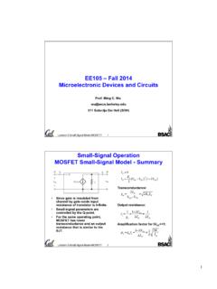
EE105 – Fall 2014 Microelectronic Devices and Circuits
inst.eecs.berkeley.eduDrain current depends on threshold voltage which in turn depends on v SB. Back-gate transconductance is: 0 < η < 3 is called the back-gate transconductance parameter. bulk terminal is a reverse-biased diode. Hence, no conductance from the bulk terminal to other terminals. Lecture13-Small Signal Model-MOSFET 4 MOSFET Small-Signal Operation