Electrons And Holes In Semiconductors
Found 7 free book(s)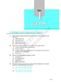
SOLID SSOLID SSOLID SSOLID STTTAAATETETETETE
ncert.nic.inholes. (ii) Holes will appear to be moving towards the negatively charged plate. (iii) Both electrons and holes appear to move towards the positively charged plate. (iv) Movement of electrons is not related to the movement of holes. 43. Which of the following statements are true about semiconductors?

Field Effect Transistors
learnabout-electronics.orgSEMICONDUCTORS 3.PDF 1 E. COATES 2016 . Field Effect Transistors Module 4.1 Junction Field Effect Transistors Field Effect Transistors ... the bipolar devices in which both holes and electrons are responsible for current flow in any one device. The JFET This was the earliest FET device available. It is a
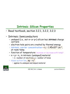
Intrinsic Silicon Properties
www.egr.msu.eduConduction in Semiconductors • doping provides free charge carriers, alters conductivity ... electrons more mobile than holes ⇒conductivity of n+ > p+ l t w A Mobility often assumed constant but is a function of Temperature and Doping Concentration. ECE 410, Prof. A. Mason Lecture Notes 6.4

Chapter 2 Semiconductor Heterostructures
courses.cit.cornell.eduSimilarly, there are more holes in the region x 0 (where p ppo Na) than in the region x 0 (where d i no N n p p 2 2 ). Consequently, electrons will diffuse from the n-side into the p-side and holes will diffuse from the p-side into the n-side. Electrons on the n …

Physics Notes Class 12 Chapter 14 Semiconductor ...
ncerthelp.comare the number density of electrons and holes and n i is number density of intrinsic carriers, i.e., electrons or holes. In n-type semiconductor, n e > > n h In p -type semiconductor, n h > > n e Electrical conductivity of extrinsic semiconductor is given by σ = 1 / ρ = e (n e μ e + n h μ h) where ρ is resistivity, μ e and μ h

Semiconductor Diodes - Learn About Electronics
www.learnabout-electronics.orgsilicon now has a shortage of valence electrons in its structure, which can also be considered to be a surplus of ‘holes’ or positive charge carriers, whereas the N type layer is doped with atoms having five electrons in its valence shell and therefore has a surplus of electrons, which are negative charge carriers. Diode PN Junction

THERMOELECTRIC REFRIGERATION - Engr. Adnan Qamar
engineersedge.weebly.comcreates “holes”. P doped semiconductors are positive charge carriers. There’s an appearance that a hole is moving when there is a current applied because an electron moves to fill a hole, creating a new hole where the electron was originally. …