Emitter Ii
Found 10 free book(s)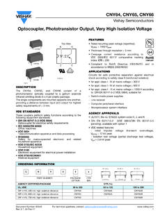
Optocoupler, Phototransistor Output, Very High Isolation ...
www.vishay.comCollector emitter voltage IC = 1 mA VCEO 32 V Emitter collector voltage IE = 100 μA VECO 7V Collector emitter leakage current VCE = 20 V, IF = 0 A ICEO 200 nA COUPLER Collector emitter saturation voltage IF = 10 mA, IC = 1 mA VCEsat 0.3 V Cut-off frequency VCE = 5 V, IF = 10 mA, RL = 100 fc 110 kHz Coupling capacitance f = 1 MHz Ck 0.3 pF

Optocoupler, Phototransistor Output, AC Input, Single ...
www.vishay.comCollector emitter voltage IC = 100 μA VCEO 70 - - V Emitter collector voltage IE = 100 μA VECO 7- - V Collector dark current VCE = 20 V, IF = 0 ICEO-- 100 nA COUPLER Collector emitter saturation voltage IF = ± 10 mA, IC = 1 mA VCEsat-- 0.3 V Cut-off frequency VCE = 5 V, IF = ± 10 mA, RL = 100 Ω fc - 100 - kHz Capacitance (input to output ...

MJE13003 - SWITCHMODE Series NPN Silicon Power Transistor
www.onsemi.comFigure 3. Base−Emitter Voltage Figure 4. Collector−Emitter Saturation Region Figure 5. Collector Cutoff Region 2 0.8 104 VBE, BASE−EMITTER VOLTAGE (VOLTS) 10−1 0 TJ = 25°C TJ = 150°C 20 0.07 0.3 −0.4 Figure 6. Capacitance 500 VR, REVERSE VOLTAGE (VOLTS) Cib 0.1, COLLECTOR CURRENT (A)μ I C 0.05 103 102 101 100 −0.2 +0.2 +0.4 +0.6 ...

Transistors: Bipolar Junction Transistors (BJT)
ocw.mit.eduWith the voltage and as shown, the Base-Emitter (B-E) junction is forward biased and the Base-Collector (B-C) junction is reverse biased. VBE VCB The current through the B-E junction is related to the B-E voltage as (VVBE / T 1) IIEs= e− (1.1) Due to the large differences in the doping concentrations of the emitter and the base regions

Lecture 10 Emitter Follower (Common Collector Amplifier)
inst.eecs.berkeley.edu2/23/2008 EE105 Fall 2007 1 Lecture 10 OUTLINE • BJT Amplifiers (3) – Emitter follower (Common-collector amplifier) EE105Spring2008 Lecture10,Slide1Prof.Wu,UC Berkeley
Basic Electronics - New York University
engineering.nyu.eduNPN BJT: How it works — II • If a positive voltage (>0.6V) is applied to the base of an npn transistor, the pn junction between the base and emitter becomes forward-biased. During forward bias, escaping electrons are drawn to the positive base. • Some electrons exit through the base, but because the p-type base

BJT Amplifiers 6 - Pearson
www.pearsonhighered.comThe sinusoidal collector-to-emitter voltage varies above and below its Q-point value, V CEQ, 1808 out of phase with the base voltage, as illustrated in Figure 6–2. A transistor always produces a phase inversion between the base voltage and the collector voltage. A Graphical Picture The operation just described can be illustrated graphically ...

Chapter 4 BJT BIASING CIRCUIT
site.iugaza.edu.psI II E =+≅ ( 1)β BC V VV ... The addition of the emitter resistor to the dc bias of the BJT provides improved stability, that is, the dc bias currents and voltages remain closer to where they were set by the circuit when outside conditions, such as temperature, and

Food wastage footprint: Impacts on natural resources ...
www.fao.orgtop emitter after USA and China. Globally, the blue water footprint (i.e. the consumption of surface and groundwater resources) of food wastage is about 250 km 3, which is equivalent to the annual water dis - charge of the Volga river, or three times the volume of lake Geneva. Finally, produced but uneaten food

Report of the Conference of the Parties on its twenty ...
unfccc.intII. Organizational matters (Agenda item 2) A. Election of the President of the Conference of the Parties at its twenty-first session (Agenda sub-item 2(a)) 3. At the 1st meeting of the COP,3 on 30 November, the President of COP 20, Mr. Pulgar-Vidal, recalled that, in accordance with rule 22, paragraph 1, of the draft rules ...