Search results with tag "Biasing"

Scaling and Biasing Analog Signals - symres.com
www.symres.comScaling and Biasing Analog Signals November 2007 Introduction Scaling and biasing the range and offset of analog signals is a useful skill for working
Chapter 6 FET Biasing - Khon Kaen University
home.kku.ac.thChapter 6 FET Biasing Chapter 6 FET Biasing 1 INTRODUCTION The general relationships that can be applied to the dc analysis of all FET amplifiers are and For JFETs and depletion-type MOSFETs, Shockley’s equation is applied to relate the input and output quantities: For enhancement-type MOSFETs, the following equation is applicable:

1 Audio Amplifiers 2 Buffer Amplifiers/Driving Cap Loads 3 ...
www.analog.comcircuit, the amplifier biasing must also be noiseless, that is free from noise added directly or indirectly by the biasing (see Reference 1). Resistors with DC across them should have low excess noise (film types), or be AC-bypassed. Thus R1, R2, R3, R4, R7, and R8 are preferably metal films, with R7-R8 bypassed.
CRYSTAL OSCILLATOR CIRCUITS
bgaudioclub.org7.6. Butler Harmonic Circuits, C-tap89 7.7. Butler Harmonic Circuits, L-tap93 6. TRIMMING THE CRYSTAL FREQUENCY101 9. THE START-UP PROBLEM 103 9.1. Biasing ICs 103 9.2. Biasing Discrete Transistors 105 10. DISCRETE TRANSISTOR OSCILLATORS 109 A. Circuit Selection and Testing109 B. Fundamental Circuits 111 10.1. Miller-FET 111 10.2. Miller ...

Transistor Biasing - Talking Electronics
www.talkingelectronics.comTransistor Biasing 195 Fig. 9.4 When VCE is too low (less than 0.5V for Ge transistors and 1V for Si transistors), the collector- base junction is not properly reverse biased.

Lockin Amplifier - MIT
web.mit.eduThe rest of the schematic above is just biasing and base driving. R8, C1, and R9 create a stable reference voltage. The resistors around U1 create a summing amplifier, and the resistors around U2 an inverting amplifier, so that the base voltages V B1 and V B2 have a

Differential ADC Biasing Techniques, Tips and Tricks
ww1.microchip.com2002 Microchip Technology Inc. DS00842A-page 3 AN842 FIGURE 4: Actual input showing amplifier limitations. In the circuit of Figure 5, a 2.048 V REF is used to …
Abstract for Experimental Methods in RF Design - W7ZOI
w7zoi.nettransistor. The large signal model is now applied, used to analyze methods for biasing the part. Similar discussions are presented for the junction field

Meeting Biasing Requirements of Externally Biased RF ...
www.analog.comAPPLICATION NOTE AN-1363 Rev. A | Page 3 of 16 BIASED AMPLIFIERS POWER SUPPLY SEQUENCING Power supply sequencing is critical while operating externally
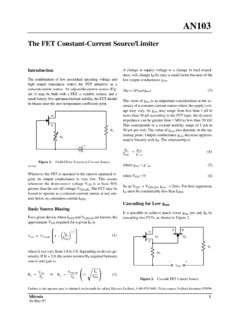
The FET Constant-Current Source/Limiter
www.vishay.comAN103 Siliconix 10-Mar-97 5 Choosing the Correct JFET for Source Biasing Each of the Siliconix device data sheets include typical transfer curves that …

Application Note 847 FAILSAFE Biasing of Differential Buses
www.ti.comSERIAL PROTOCOL Apopular format for low speed data transmission is an asyn-chronous protocol. A typical format is composed of 12 bits. The start bit initiates the timing sequence.
Generating Sequences With Recurrent Neural Networks
arxiv.orgA method for biasing the samples towards higher probability (and greater legibility) is described, along with a technique for ‘priming’ the sam-ples on real data and thereby mimicking a particular writer’s style. Finally, concluding remarks and directions for future work are given in Section 6.

Chapter 4 Junction Field Effect Transistor Theory and ...
staff.utar.edu.my4.1 Biasing the JFET In normal operation, the gate of JFET is always reverse-biased. Thus, an n-channel type, the gate is biased with negative voltage i.e. gate voltage is less than zero volt V G < 0, whilst for p-channel type, the gate is biased with positive voltage i.e. gate voltage is greater than zero voltage V …

II PU Midterm Exam Syllabus November 2021
www.jaincollege.ac.in2. Bipolar Junction Transistor (BJT) Biasing 3. Transistor Amplifiers 4. 10. Digital Electronics TERM – II [ Analog Electronics] 1. Field Effect Transistor (FET) Feedback in Amplifiers 5. Operational amplifier (Op-Amp) 6. Oscillators FRENCH 1.Tenses (présent, futur proche, passe récent, passe compose, imparfait, future simple, présent ...

Chapter 4 BJT BIASING CIRCUIT
site.iugaza.edu.psI II E =+≅ ( 1)β BC V VV ... The addition of the emitter resistor to the dc bias of the BJT provides improved stability, that is, the dc bias currents and voltages remain closer to where they were set by the circuit when outside conditions, such as temperature, and

MC1496, MC1496B Balanced Modulators/ Demodulators
www.onsemi.comparticular circuit and biasing conditions chosen. Power Dissipation Power dissipation, PD, within the integrated circuit package should be calculated as the summation of the voltage−current products at each port, i.e. assuming V12 = V6, I5 = I6 = I12 and ignoring base current, PD = 2 I5 (V6 − V14) + I5)V5 − V14 where subscripts refer to ...
Lecture 17: Clock Recovery - Stanford University
web.stanford.edu• FET’s are non-linear but what we really need is to clamp the swing. Also if load transfer function is symmetric CMRR is improved [19] • Use replica feedback biasing to cancel substrate and supply noise Sum of transistor I-V and diode-connected I-V curve Ids Vds Vctrl @ various V ctrl Vbias Vctrl i+ i-o- o+-+ Replica loop k eeps the s wing

Audio Power Amplifier - de Smith
www.desmith.netChapter 6 The output stage II Distortion number 4: VAS loading distortion ... The biasing requirements The linearity issues of series Class-G The static linearity ... Chapter 12 FET output stages The characteristics of power FETS FET versus BJT output stages Advantages of FETs
MOSFET Device Physics and Operation
homepages.rpi.eduindependent of the biasing conditions. However, between the semiconductor and the metal contact, the Fermi level is shifted by E Fm – E Fs = qV (see Figure 1.3(b)). Hence, we have a quasi-equilibrium situation in which the semiconductor can be treated as if in thermal equilibrium. A MOS structure with a p-type semiconductor will enter the ...

Biasing GaN on SiC HEMT Devices - RFMW Ltd, …
www.rfmw.comBiasing GaN on SiC HEMT Devices . DC biasing of GaN HEMT devices is very similar to GaAs pHEMT devices – they are both N-channel depletion mode transistors with 0.25um gate lengths.
Similar queries
Scaling and Biasing Analog Signals, Scaling and biasing, Chapter 6 FET Biasing, Chapter 6 FET Biasing Chapter 6 FET Biasing, Circuit, Biasing, Transistor Biasing, Collector, Lockin Amplifier, Differential ADC Biasing Techniques, Tips and Tricks, Abstract for Experimental Methods in, Signal model, Meeting Biasing Requirements of Externally Biased, AMPLIFIERS, FET Constant-Current Source/Limiter, JFET, Application Note 847 FAILSAFE Biasing of Differential Buses, Generating Sequences With Recurrent Neural, BIASING CIRCUIT, Emitter, Chapter 6, Chapter, Biasing GaN on SiC HEMT Devices