Ion Implantation
Found 8 free book(s)
Simultaneous Removal of Particles from Front and Back ...
www.akrionsystems.comElectrostatic chuck (ESC) mark is a common backside contamination and remains after a variety of micro-fabrication processes such as lithography, ion implantation, plasma etch, film deposition,

Ion implantation in silicon technology - Axcelis.com
www.axcelis.com14 The Industrial Physicist the sloping lines in Figure 2. Implantation is actually extremely inefficient at modifying material composition. The highest ion dose implanted with an economical
4 Contamination monitoring and analysis in semiconductor ...
cdn.intechweb.orgContamination monitoring and analysis in semiconductor manufacturing 59 second part of this chapter will consider the particle monitoring on bare wafers and

Trident Tritaniu m Ace tabular System Surgical Protocol
www.bizwan.com1 Trident® Tritaniu m® Acetabular System Surgical Protocol This publication sets forth detailed recommended procedures for using Stryker Orthopaedics devices and instruments.

Surlyn - DuPont
www.dupont.com3URGXFW,QIRUPDWLRQ 3URGXFWDQG3URSHUWLHV2YHUYLHZ Surlyn ® thermoplastic resins Basic Description DuPont Surlyn brand resins are unique ionomer- class molding and extrusion materials created
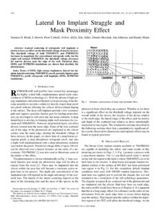
Lateral ion implant straggle and mask proximity effect ...
www.qed2.comHOOK et al.: LATERAL ION IMPLANT STRAGGLE AND MASK PROXIMITY EFFECT 1947 Fig. 2. Contour plot of simulated doping near resist mask edge. Only boron

SRIM Tutorial 1 - Ion Ranges, Doses and Damage
www.srim.orgPage 1 of 6 Tutorial #1- Introduction to Ion Ranges, Doses and Damage This Tutorial will cover how to find the energy and dose of ions required to implant atoms into a

20160317 mppc kapd9005e01 - Hamamatsu Photonics
www.hamamatsu.com2 - Considering silicon’s narrow bandgap (1.14 eV) and due to higher transition probability of a photoelectron from a silicon crystal’s valence band to its conduction band than emission probability of a photoelectron from an