Mos Transistors
Found 10 free book(s)
3. Short Channel Effects on MOS Transistors.
csit-sun.pub.rovariations in MOS transistors and mismatches in the emitter areas of bipolar devices. 3: Short Channel Effects 19 Institute of Microelectronic Systems Impact of Device Variations. 1.10 1.20 1.30 1.40 1.50 1.60 Leff (in mm) 1.50 1.70 1.90 2.10 Dela y …

8. MOS Transistors, CMOS Logic Circuits
web.stanford.eduMOS Transistors, CMOS Logic Circuits, and Cheap, Powerful Computers. M. Horowitz, J. Plummer, R. Howe 2 Reading • Chapter 4 in the reader • For more details look at –A&L 5.1 Digital Signals (goes in much more detail than we need) –A&L 6-6.3 MOS Devices. M. Horowitz, J. Plummer, R. Howe 3
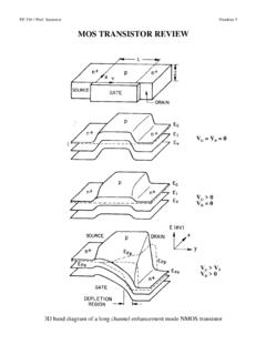
MOS TRANSISTOR REVIEW
web.stanford.eduMOS Device Scaling Na P N+ N+ L xox Xj o l P N+ S G D Scaled MOS Transistor Why do we scale MOS transistors? 1. Increase device packing density 2. Improve frequency response (transit time) α 1 L 3. Improve current drive (transconductance gm) g I V V const W L K t V V linear region W L K t V V V saturation region m D G D n ox ox DD n ox ox GT D ...

Lecture 15: MOS Transistor models: Body effects, SPICE models
inst.eecs.berkeley.edumodes of operation of a MOS FET: – Voltage controlled resistor model – I-V curve (Square-Law Model) – Saturation model In this lecture, we will: – add a correction due to the changing depletion region, called the body effect – Produce small signal models for the FET – and look at how MOS Transistors are modeled in SPICE

5 MOS Field-Effect Transistors (MOSFETs)
learninglink.oup.com5 MOS Field-Effect Transistors (MOSFETs) Section 5.1: Device Structure and Physical Operation 5.1 An NMOS transistor is fabricated in a 0.13-µm CMOS process with L = 1.5Lmin and W = 1.3 µm. The process technology is specified to have tox =2.7nm, μn =400cm2/V·s, and Vtn =0.4V. (a) Find Cox, kn,andkn. (b) Find the overdrive voltage VOV and ...
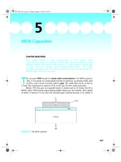
MOS Capacitor - Chenming Hu
www.chu.berkeley.eduadvanced transistors (see Section 7.4). The MOS capacitor is not a widely used device in itself. However, it is part of the MOS transistor—the topic of the next tw o chapters. The MOS transistor is by far the most widely used semiconductor device. An MOS transistor (Fig. 5–2) is an MOS capacitor with two PN junctions flanking the capacitor.

MOS Transistor Theory
people.ee.duke.eduMOS Transistor Theory • So far, we have viewed a MOS transistor as an ideal switch (digital operation) – Reality: less than ideal. EE 261 James Morizio 2. EE 261 James Morizio 3 Introduction • So far, we have treated transistors as ideal switches • An ON transistor passes a finite amount of current – Depends on terminal voltages ...
Dynamic Combinational Circuits
people.ee.duke.edu– Transistors are leaky (I OFF „ 0) – Dynamic value will leak away over time – Formerly miliseconds, now nanoseconds! • Use keeper to hold dynamic node – Must be weak enough not to fight evaluation A f H 2 2 1 k X Y weak keeper. James Morizio 15 Charge Sharing (redistribution) Mp M e VDD Out A
Lecture 24 MOSFET Basics (Understanding with no math ...
alan.ece.gatech.edun-channel MOS Transistor G=Gate, D=Drain, S=Source, B=Body (substrate, but to avoid confusion with substrate, B is used) G S D B V SG V SB V SD---+ p-channel MOS Transistor Note: All voltages are shown in their “positive “ direction. Obviously, V YX =-V XY for any voltage MOS Transistor Qualitative Description
MOS Transistor - Chenming Hu
www.chu.berkeley.eduMOS Transistor CHAPTER OBJECTIVES This chapter provides a comprehensive introduction to the modern MOSFETs in their on state. (The off state theory is the subject of the next chapter.) It covers the topics of surface mobility, body effect, a simple IV theory, and a more complete theory applicable to both long- and short-channel MOSFETs.