Search results with tag "Mos transistors"

8. MOS Transistors, CMOS Logic Circuits
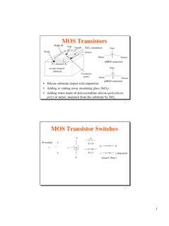
web.stanford.eduMOSFET a.k.a. MOS Transistor • Are very interesting devices –Come in two “flavors” –pMOSand nMOS –Symbols and equivalent circuits shown below • Gate terminal takes no current (at least no DC current) –The gate voltage*controls whether the “switch” is ON or OFF pMOS nMOS R on gate * actually, the gate –to –source voltage ...

3. Short Channel Effects on MOS Transistors.
csit-sun.pub.rovariations in MOS transistors and mismatches in the emitter areas of bipolar devices. 3: Short Channel Effects 19 Institute of Microelectronic Systems Impact of Device Variations. 1.10 1.20 1.30 1.40 1.50 1.60 Leff (in mm) 1.50 1.70 1.90 2.10 Dela y …

Lecture11-MOS Cap Delay
bwrcs.eecs.berkeley.eduMOS Transistor as a Switch Saw that real transistors aren’t exactly resistors Look more like current sources in saturation Two questions: Which region of IV curve determines delay? How can that match up with the RC model? EE141 29 EECS141 Lecture #11 29 Transistor Driving a Capacitor • With a step input: ID VDS VDD /2 VDD VDD ÆVDD/2 VGS ...

Lecture 15: MOS Transistor models: Body effects, SPICE models
inst.eecs.berkeley.edutransistor (BJT): Chapter 7 zThen go on to design of transistor amplifiers: chapter 8 Department of EECS University of California, Berkeley EECS 105 Spring 2004, Lecture 15 Prof. J. S. Smith MOS operation zAn inversion mode MOS transistor operates by producing a sheet carriers just under the oxide zThe names source and drain are picked so that the
MOS Transistors - Duke Electrical and Computer Engineering
people.ee.duke.edu– Pull-up circuit corresponds to pull-up graph 11 21 Graph Models a b c Gnd d a b d c Pull-down circuit Gnd ... Gate-Level Mux Design • How many transistors are needed? 20 14 27 ... e.g. VHDL, Verilog • Example: Consider the carry function c o = ab + bc + c i a 22 43
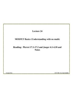
Lecture 24 MOSFET Basics (Understanding with no math ...
alan.ece.gatech.eduMOS Transistor Qualitative Description Assume an n-channel (receives it’s name from the “type” of channel present when current is flowing) device with its source and substrate grounded (i. e., V S =V B =0 V). For any value of V DS: •when V GS <0 (accumulation), the source to drain path consists of two back to back diodes.
Lecture 12: MOS Transistor Models
inst.eecs.berkeley.eduCurrent in transistor is very low until the gate voltage crosses the threshold voltage of device (same threshold voltage as MOS capacitor) Current increases rapidly at first and then it finally reaches a point where it simply increases linearly VGS IDS VT VGS IDS VDS

MOS Transistor Theory
people.ee.duke.eduMOS Transistor Theory • Study conducting channel between source and drain • Modulated by voltage applied to the gate (voltage-controlled device) • nMOS transistor: majority carriers are electrons (greater mobility), p-substrate doped (positively doped) • pMOS transistor: majority carriers are holes (less
MOS Transistor - Chenming Hu
www.chu.berkeley.eduMOS Transistor CHAPTER OBJECTIVES This chapter provides a comprehensive introduction to the modern MOSFETs in their on state. (The off state theory is the subject of the next chapter.) It covers the topics of surface mobility, body effect, a simple IV theory, and a more complete theory applicable to both long- and short-channel MOSFETs.
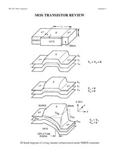
MOS TRANSISTOR REVIEW - Stanford University
web.stanford.eduMOS Transistor 5 In reality constant field scaling has not been observed strictly. Since the transistor current is proportional to the gate overdrive (VG-VT), high performance demands have dictated the use of higher supply voltage. However, higher supply voltage implies increased power dissipation (CV2f). In the recent past low power ...