Transcription of 8. MOS Transistors, CMOS Logic Circuits
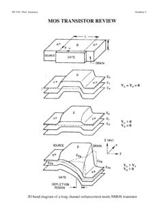
1 M. Horowitz, J. Plummer, R. Howe1E40 MMOS Transistors, CMOS Logic Circuits ,and Cheap, Powerful ComputersM. Horowitz, J. Plummer, R. Howe2 Reading Chapter 4 in the reader For more details look at A& Signals (goes in much more detail than we need) A& DevicesM. Horowitz, J. Plummer, R. Howe3 MOSFET MOS transistor Are very interesting devices Come in two flavors pMOSand nMOS Symbols and equivalent Circuits shown below Gate terminal takes no current (at least no DC current) The gate voltage*controls whether the switch is ON or OFFpMOSnMOSR ongategate* actually, the gate to source voltage, VGSM. Horowitz, J. Plummer, R. Howe4nMOSi-V Characteristics nMOSis still a device Defined by its relationship between current and voltage But it has 3 terminals! Current only flows between the source and drain No current flows into the gate terminal!
2 VDSiDSGDSviRemember the resistor?M. Horowitz, J. Plummer, R. Howe5 SimpleModel of an nMOSD evice We will model an nMOSdevice by components we know Resistor Switch NMOSS ource = GndGate = Gnd=> OffGate = Vdd=> On This really simple model issuitable for applications wherethere s one value of On Horowitz, J. Plummer, R. Howe6 How Does an nMOST ransistor Actually Work?(FYI not essential for this course) + Horowitz, J. Plummer, R. Howe7 Problem With nMOSD evice While an nMOSdevice makes a great switch to Gnd It doesn t work that well if we want to connect to Vdd To turn transistor on Gate needs to be higher than source But we want the source to be at Vdd Oops ..M. Horowitz, J. Plummer, R. Howe8pMOSiDSvs. VDSC haracteristics Similar to nMOS, but upside down! Turns on when the gate-to-source voltage is < -1 V And the drain-to-source voltage should be negative Source should be the terminal with the higher voltage!
3 VDSiDSGSDM. Horowitz, J. Plummer, R. Howe9 SimpleModel of a pMOSD evice We will model an pMOSdevice by components we know Resistor Switch NMOSS ource = VddGate = Gnd=> OnGate = Vdd=> OffVDSiDSOnOffM. Horowitz, J. Plummer, R. Howe10 How Does a pMOST ransistor Actually Work?(FYI not part of this course) M. Horowitz, J. Plummer, R. Howe11nMOSand pMOSD evices Complement Each Other Complementary MOS or CMOS PMOSS ource = Vdd(+ supply)Gate = Gnd=> OnGate = Vdd=> Off NMOSS ource = GndGate = Gnd=> OffGate = Vdd=> OnRonM. Horowitz, J. Plummer, R. Howe12 MOST ransistor Summary mos transistors are extremelyusefuldevices Almost all of your electronics usesthem on the inside Including your phone, laptop, WiFiand Bluetooth, and your Arduino Come in two flavors nMOS It is a switch which connects source to drain If the gate-to-source voltage is greater than Vth(around 1 V) Positive gate-to-source voltages turn the device on.
4 pmos It is a switch which connects source to drain If the gate-to-source voltage is less than Vth(around -1 V) Negative gate-to-source voltages turn the device there s zero current into the gate!M. Horowitz, J. Plummer, R. Howe13 MOS Logic GatesM. Horowitz, J. Plummer, R. Howe14 What Does This Circuit Do? Is the output a Logic function of the input? Consider Vin= GNDInOutVDDpMOSnMOSM. Horowitz, J. Plummer, R. Howe15 What Does This Circuit Do? Now consider Vin= VDDInOutVDDpMOSnMOSM. Horowitz, J. Plummer, R. Howe16 Building Logic Gates from mos transistors Remember BooleanLogic? AND,OR NAND = Not-AND = AND followed by Inverter Outputis only low when A and B are true (high) NOR= Not-OR = OR followed by Inverter Outputis low when either A or B is true (high) Youcan make them from MOS devices But only the inverting gates (NOR and NAND)M.
5 Horowitz, J. Plummer, R. Howe17 Building a CMOS NAND Gate Output should be low if both input are high (true) Output should be high if either input is low (false)M. Horowitz, J. Plummer, R. Howe18 LogicSymbolsM. Horowitz, J. Plummer, R. Howe19If You Look At Your Computer Chip It is just billions of transistors Creating many Logic gates, and memory Take EE108A if you want know how we do Horowitz, J. Plummer, R. Howe20 HOW THE MOS TRANSISTORCHANGED THE WORLD ..M. Horowitz, J. Plummer, R. Howe21 First Computing Machines Were MechanicalPicture of a version of the Babbage difference engine built by the Museum of Science, UK The calculating section of Difference Engine No. 2, has 4,000 moving parts (excluding the printing mechanism) and weighs tons. It is seven feet high, eleven feet long and eighteen inches in depth M.
6 Horowitz, J. Plummer, R. Howe22 Moving Electrons is Easier than Moving Metal Building electronics: Started with tubes, then miniature tubes Transistors, then miniature transistors Components were getting cheaper, more reliable but: There is a minimum cost of a component (storage, handling ..) Total system cost was proportional to complexity Integrated Circuits changed that Printed a circuit, like you print a picture, Create components in parallel Cost no longer depended on # of devicesM. Horowitz, J. Plummer, R. Howe231stIntegrated CircuitJack Kilby, Nobel Laureate in Physics 2000 Bob Noyce1st(Bipolar Junction) transistor Christmas Eve 1947By Bardeen, Brattain, and Shockley, Nobel Laureates in Physics 1956( )(Courtesy of TI and Huff, SEMATECH)19581947A Little HistoryM. Horowitz, J. Plummer, R.
7 Howe24 What is an Integrated Circuit? A device having multiple electrical components and their interconnects manufactured on a single substrate. First IC 1958 Jack Kilbyat TI Germanium A hack Wax support Made history Planar Process 1961 Bob Noyceat Fairchild SiliconImage from State of the Art Stan AugartenM. Horowitz, J. Plummer, R. Howe251 Introduction -Chapter 1 SILICON VLSI TECHNOLOGYF undamentals, Practice and ModelingBy Plummer, Deal & Griffin 2000 by Prentice HallUpper Saddle River NJINTRODUCTION -Chapter 1 in the Text This course is basically about silicon chip fabrication, the technologies used to manufacture ICs. We will place a special emphasis on computer simulation tools to help understand these processes and as design tools. These simulation tools are more sophisticated in some technology areas than in others, but in all areas they have made tremendous progress in recent years.
8 1960 and 1990 integrated Circuits . Progress due to: Feature size reduction years (Moore s Law).Increasing chip size -? 16% per year. Creativity in implementing Contact TransistorFirst Integrated CircuitModern Microprocessor1 Introduction -Chapter 1 SILICON VLSI TECHNOLOGYF undamentals, Practice and ModelingBy Plummer, Deal & Griffin 2000 by Prentice HallUpper Saddle River NJINTRODUCTION -Chapter 1 in the Text This course is basically about silicon chip fabrication, the technologies used to manufacture ICs. We will place a special emphasis on computer simulation tools to help understand these processes and as design tools. These simulation tools are more sophisticated in some technology areas than in others, but in all areas they have made tremendous progress in recent years. 1960 and 1990 integrated Circuits .
9 Progress due to: Feature size reduction years (Moore s Law).Increasing chip size -? 16% per year. Creativity in implementing ThisTo ThisTo ThisMiniaturization Progress Over 50 Years Modern silicon chipshave > 109components in 1 cm2area. M. Horowitz, J. Plummer, R. Howe261965 -Moore Intel MicroprocessorsMoore s Law The complexity for minimum component costs has increased at a rate of roughly a factor of 2 per year. Gordon Moore, 1965M. Horowitz, J. Plummer, R. Howe27 Transistors per mm2 KaizadMistry, Intel Technology and Manufacturing Day, March 28, 2017M. Horowitz, J. Plummer, R. Howe28 What This Means1985 (Intel 80386)275,000 transistors104 mm2; 2640 Tr/mm21989 (Intel 80486)1,180,235 transistors16,170 Tr/mm2 Intel 10 nm CMOS*circa 2019100,000,000 the original chip area could contain > 10 billion transistors!
10 80386 chip areashrinks to 17 mm280386 die sizeshrinks to mm2*KaizadMistry, Intel Technology and Manufacturing Day, March 28, 2017 Chip edge is only twice thediameter of a human hair! M. Horowitz, J. Plummer, R. Howe29 Take The Cover Off A MicroprocessorPackaged dieCross-sectionSingle transistorFull wafer (100s of dies)modern wafers: 200-300 mm diameter (8-12 inches)M. Horowitz, J. Plummer, R. Howe30 Learning Objectives Understand how nMOSand pMOStransistor work Voltage controlled switch, the gate voltage controls whether the switch is ON of OFF nMOSdevices connect output to Gnd pMOSdevices connect the output to Vdd Be able to create MOS NAND, NOR and Inverter Circuits Using pMOSand nMOSdevices