Transcription of Bipolar Transistor
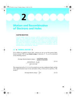
1 Page 291 Friday, February 13, 2009 4:01 PM. 8. Bipolar Transistor CHAPTER OBJECTIVES. This chapter introduces the Bipolar junction Transistor (BJT) operation and then presents the theory of the Bipolar Transistor I-V characteristics, current gain, and output conductance. High-level injection and heavy doping induced band narrowing are introduced. SiGe Transistor , transit time, and cutoff frequency are explained. Several Bipolar Transistor models are introduced, , Ebers Moll model, small-signal model, and charge control model. Each model has its own areas of applications. T. he Bipolar junction Transistor or BJT was invented in 1948 at Bell Telephone Laboratories, New Jersey, USA. It was the first mass produced Transistor , ahead of the MOS field-effect Transistor (MOSFET) by a decade.
2 After the introduction of metal - oxide -semiconductor (MOS) ICs around 1968, the high- density and low-power advantages of the MOS technology steadily eroded the BJT's early dominance. BJTs are still preferred in some high-frequency and analog applications because of their high speed, low noise, and high output power advantages such as in some cell phone amplifier circuits. When they are used, a small number of BJTs are integrated into a high-density complementary MOS. (CMOS) chip. Integration of BJT and CMOS is known as the BiCMOS. technology. The term Bipolar refers to the fact that both electrons and holes are involved in the operation of a BJT. In fact, minority carrier diffusion plays the leading role just as in the PN junction diode. The word junction refers to the fact that PN junc- tions are critical to the operation of the BJT.
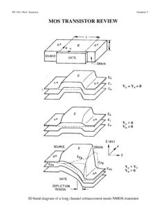
3 BJTs are also simply known as Bipolar transistors. INTRODUCTION TO THE BJT . A BJT is made of a heavily doped emitter (see Fig. 8 1a), a P-type base, and an N-type collector. This device is an NPN BJT. (A PNP BJT would have a P+ emitter, N-type base, and P-type collector.) NPN transistors exhibit higher transconductance and 291. Page 292 Friday, February 13, 2009 4:01 PM. 292 Chapter 8 Bipolar Transistor E N P N C. Emitter Base Collector B. VBE VCB. (a). Ec . EFn VBE EFp . Ev VCB. EFn (b). Ic VBE. 0 VCB. (c). FIGURE 8 1 (a) Schematic NPN BJT and normal voltage polarities; (b) electron injection from emitter into base produces and determines IC ; and (c) IC is basically determined by VBE and is insensitive to VCB. speed than PNP transistors because the electron mobility is larger than the hole mobility.
4 BJTs are almost exclusively of the NPN type since high performance is BJTs'. competitive edge over MOSFETs. Figure 8 1b shows that when the base emitter junction is forward biased, electrons are injected into the more lightly doped base. They diffuse across the base to the reverse-biased base collector junction (edge of the depletion layer). and get swept into the collector. This produces a collector current, IC. IC is independent of VCB as long as VCB is a reverse bias (or a small forward bias, as explained in Section ). Rather, IC is determined by the rate of electron injection from the emitter into the base, , determined by VBE. You may recall from the PN diode theory that the rate of injection is proportional to eqV BE kT . These facts are obvious in Fig. 8 1c.
5 Figure 8 2a shows that the emitter is often connected to ground. (The emitter and collector are the equivalents of source and drain of a MOSFET. The base is the equivalent of the gate.) Therefore, the IC curve is usually plotted against VCE as shown in Fig. 8 2b. For VCE higher than about V, Fig. 8 2b is identical to Fig. 8 1c but with a shift to the right because VCE = VCB + VBE. Below VCE V, Page 293 Friday, February 13, 2009 4:01 PM. Collector Current 293. E C IC. VBE. N P N. IC. B. IB VCE. VBE. VCE. 0. (a) (b). IC Vcc IB. Vout IB. VCE. 0. (c) (d). FIGURE 8 2 (a) Common-emitter convention; (b) IC vs. VCE; (c) IB may be used as the parameter instead of VBE; and (d) circuit symbol of an NPN BJT and an inverter circuit. the base collector junction is strongly forward biased and IC decreases as explained in Section Because of the parasitic IR drops, it is difficult to accurately ascertain the true base emitter junction voltage.
6 For this reason, the easily measurable base current, IB , is commonly used as the variable parameter in lieu of VBE (as shown in Fig. 8 2c). We will see later that IC is proportional to IB. COLLECTOR CURRENT . The collector current is the output current of a BJT. Applying the electron diffusion equation [Eq. ( )] to the base region, 2. d n' n'. ----------- = ------- ( ). 2 2. dx LB. L B BD B ( ). Depletion layers N P N. Emitter Base Collector x 0 WB. FIGURE 8 3 x = 0 is the edge of the BE junction depletion layer. WB is the width of the base neutral region. Page 294 Friday, February 13, 2009 4:01 PM. 294 Chapter 8 Bipolar Transistor B and DB are the recombination lifetime and the minority carrier (electron). diffusion constant in the base, respectively. The boundary conditions are [Eq.]
7 ( )]. qVBE kT. n' ( 0 ) = n B0 ( e 1) ( ). qVBC kT. n' ( W B ) = n B0 ( e 1 ) n B0 0 ( ). where nB0 = ni2/NB , and NB is the base doping concentration. VBE is normally a forward bias (positive value) and VBC is a reverse bias (negative value). The solution of Eq. ( ) is W B x . sinh ----------------- - qVBE kT LB . n' ( x ) = n B0 ( e 1 ) ------------------------------------- ( ). sinh ( W B L B ). Equation ( ) is plotted in Fig. 8 4. Modern BJTs have base widths of about m. This is much smaller than the typical diffusion length of tens of microns (see Example 4 4 in Section ). In the case of WB << LB , Eq. ( ) reduces to a straight line as shown in Fig. 8 4. n' ( x ) = n' ( 0 ) ( 1 x W B ). 2 ( ). n iB qVBE kT. -(e = ------- 1 ) 1 -------- x . - NB W B . niB is the intrinsic carrier concentration of the base material.
8 The subscript, B, is added to ni because the base may be made of a different semiconductor (such as SiGe alloy, which has a smaller band gap and therefore a larger ni than the emitter and collector material). n'. n' (0). n2i n' = (eqVBE/kT 1). NB WB WB WB x/WB. FIGURE 8 4 When WB << LB, the excess minority carrier concentration in the base is approximately a linear function of x. Page 295 Friday, February 13, 2009 4:01 PM. Collector Current 295. As explained in the PN diode analysis, the minority-carrier current is dominated by the diffusion current. The sign of IC is defined in Fig. 8 2a and is positive. dn n' ( 0 ). I C = A EqD B ------- = A EqDB ------------- dx WB. 2 ( ). D B n iB qVBE kT. - -------- ( e = A Eq -------- 1). WB NB. AE is the area of the BJT, specifically the emitter area.
9 Notice the similarity between Eq. ( ) and the PN diode IV relation [Eq. ( )]. Both are proportional to ( e qV kT 1 ) and to Dni2/N. In fact, the only difference is that dn'/dx has produced the 1/WB term in Eq. ( ) due to the linear n' profile. Equation ( ) can be condensed to qVBE kT. IC = IS( e 1) ( ). where IS is the saturation current. Equation ( ) can be rewritten as 2. qn qV kT. I C = A E --------i- ( e BE 1) ( ). GB. In the special case of Eq. ( ). 2 2. ni NB ni p G B = ------- - -------- W B = ------- - -------- W B ( ). 2 D 2. n iB B n iB D B. where p is the majority carrier concentration in the base. It can be shown that Eq. ( ) is valid even for nonuniform base and high-level injection condition if Gb is generalized to [1]. 2. WB ni p GB ------- - -------- dx ( ).
10 2. 0 n iB D B. GB has the unusual dimension of s/cm4 and is known as the base Gummel number. In the special case of niB = ni, DB is a constant, and p(x) = NB(x) (low-level injection), 1 WB 1. G B = -------- N B( x ) dx = -------- base dopant atoms per unit area ( ). DB 0 DB. Equation ( ) illustrates that the base Gummel number is basically proportional to the base dopant density per area. The higher the base dopant density is, the lower the IC will be for a given VBE as given in Eq. ( ). The concept of a Gummel number simplifies the IC model because it [Eq. ( )] contains all the subtleties of Transistor design that affect IC: changing base material through niB(x), nonconstant DB , nonuniform base dopant concen- tration through p(x) = NB(x), and even the high-level injection condition (see Sec.)