Search results with tag "Metal oxide semiconductor"
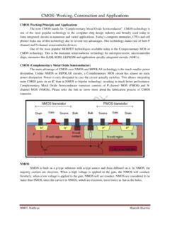
CMOS: Working, Construction and Applications
www.mpithathras.inCMOS (Complementary Metal Oxide Semiconductor) The main advantage of CMOS over NMOS and BIPOLAR technology is the much smaller power dissipation. Unlike NMOS or BIPOLAR circuits, a Complementary MOS circuit has almost no static ... There are two types of FETs: JFETs and MOSFETs. MOSFET is Metal Oxide Semiconductor Field Effect Transistor ...

Introduction to Semiconductor Technology ...
www.st.comINTRODUCTION TO SEMICONDUCTOR TECHNOLOGY 2 BASIC IC ELEMENT: THE TRANSISTOR 2.1 MOS TECHNOLOGY We will examine first the basics of MOS (Metal Oxide Semiconductor) technologies as they are used for the majority of the integrated circuits manufactured at STMicroelectronics.
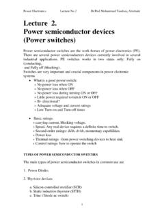
Lecture 2. Power semiconductor devices (Power switches)
www.philadelphia.edu.job. Metal oxide semiconductor field effect transistor (MOSFET) c. Insulated gate bipolar transistor (IGBT) d. Static induction transistor (SIT) 2.1 Power Diodes: These are two terminal switches, as shown in Fig. 2.1 -a, formed of a pn junction. It is not controllable and its operating states are determined by the circuit operating point.

Firmware Update Utility Manual - Samsung us
www.samsung.comCMOS stands for Complementary Metal Oxide Semiconductor. The CMOS is a semiconductor chip that is installed on the motherboard of all kinds of computer, in order to store information about system booting and setup. The CMOS can also be called the BIOS.
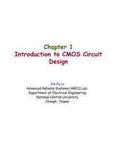
Chapter 1 Introduction to CMOS Circuit Design
www.ee.ncu.edu.twCalled metal–oxide–semiconductor (MOS) capacitor Even though gate is no longer made of metal n+ p Source DrainGate bulk Si SiO2 Polysilicon n+. ... Design Flow for a VLSI Chip Specification Behavioral Design Structural Design Physical …
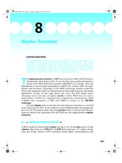
Bipolar Transistor
www.chu.berkeley.eduIt was the first mass produced transistor, ahead of the MOS field-effect transistor (MOSFET) by a decade. After the introduction of metal-oxide-semiconductor (MOS) ICs around 1968, the high-density and low-power advantages of the MOS technology steadily eroded the BJT’s early dominance. BJTs are still pref erred in some high-frequency and analog
ECE 410: VLSI Design Course Lecture Notes
www.egr.msu.eduVLSI Design Flow • VLSI – very large scale integration – lots of transistors integrated on a single chip • Top Down Design – digital mainly – coded design – ECE 411 ... – MOS = Metal Oxide Semiconductor • physical layers of the device – FET = Field Effect Transistor
MEMS Fabrication I : Process Flows and Bulk …
www-bsac.eecs.berkeley.edu2 U. Srinivasan © EE C245 IC Processing Cross-section Jaeger Masks Cross-section Masks N-type Metal Oxide Semiconductor (NMOS) process flow U. Srinivasan ©

Power MOSFET Basics
www.aosmd.comPower MOSFETs (Metal Oxide Semiconductor Field Effect Transistor) are the most commonly used power devices due to their low gate drive power, fast switching speed and superior paralleling capability. Most power MOSFETs feature a vertical structure with Source and Drain on opposite sides of the wafer in order to support higher current and voltage.

Ternary Logic Gates & Arithmetic Circuit - Ijiset
www.ijiset.comThe current technology trend is CMOS technology which is referred as Complementary Symmetry Metal Oxide Semiconductor or COSMOS. From the words
Similar queries
CMOS: Working, Construction and Applications, Metal Oxide Semiconductor, FETs, MOSFETs, Semiconductor, Samsung us, Design, Metal–oxide–semiconductor, VLSI, Transistor, Metal-oxide-semiconductor, 410: VLSI Design Course Lecture Notes, VLSI Design, Very large scale integration, Bulk, Power MOSFET, Ternary Logic Gates & Arithmetic Circuit