Transcription of Power MOSFET Basics
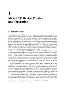
1 Source Gate Power MOSFET Basics N+. P-body Table of Contents N- Epi 1. Basic Device Structure 2. Breakdown Voltage 3. On-State Characteristics N+ Substrate 4. Capacitance 5. Gate Charge Drain 6. Gate Resistance 7. Turn-on and Turn-off Figure 1b: Planar MOSFET Structure 8. Body Diode Forward Voltage 9. Body Diode Reverse Recovery 2. Breakdown Voltage 10. Avalanche capability and ratings 11. dV/dt ratings In most Power mosfets the N+ source and P-body junction 12. Thermal Resistance Characterization are shorted through source metallization to avoid accidental 13. Power Dissipation turn-on of the parasitic bipolar transistor. When no bias is 14. Safe-Operating Area applied to the Gate, the Power MOSFET is capable of 15. Current Ratings supporting a high Drain voltage through the reverse-biased P- body and N- Epi junction.
2 In high voltage devices, most of the 1. Basic Device Structure applied voltage is supported by the lightly doped Epi layer. A. thicker and more lightly doped Epi supports higher breakdown voltage but with increased on-resistance. In lower voltage Power mosfets ( metal oxide Semiconductor Field Effect devices, the P-body doping becomes comparable to the N- Epi Transistor) are the most commonly used Power devices due to layer and supports part of the applied voltage. If the P-body is their low gate drive Power , fast switching speed and superior not designed thick or heavy enough, the depletion region can paralleling capability. Most Power mosfets feature a punch-through to the N+ source region and cause lower vertical structure with Source and Drain on opposite sides of breakdown.
3 But if it is over designed, the channel resistance the wafer in order to support higher current and voltage. and threshold voltage will also increase. So careful design of Figure 1a and 1b show the basic device structures of Trench the body and Epi doping and thickness is needed to optimize and Planar mosfets respectively. Trench mosfets are the performance. mainly used for <200V voltage rating due to their higher channel density and thus lower on-resistance. Planar In the datasheet, BVDSS is usually defined as the drain to mosfets are good for higher voltage ratings since on- source voltage when leakage current is 250uA. The leakage resistance is dominated by epi-layer resistance and high cell current flowing between source and drain is denoted by IDSS. It density is not beneficial.
4 The basic MOSFET operation is the is measured at 100% of the BVDSS rating. As temperature same for both structures. Unless specified, the N-channel increases, IDSS increases and BVDSS also increases for Power trench MOSFET is discussed in this application note. mosfets . 3. On-State Characteristics We consider here Power MOSFET under two different modes of operations: the first quadrant operation and the third N+. quadrant operation. P-body Gate First-Quadrant Operation: For an n-channel MOSFET , the device operates in the first N- Epi quadrant when a positive voltage is applied to the drain, as shown in figure 2. As the gate voltage (VG) increases above the threshold voltage (VTH), the MOSFET channel begins to N+ Substrate conduct current. The amount of current it conducts depends Drain on the on-resistance of the MOSFET , as defined by Figure 1a: Trench MOSFET Structure RDSON = VD / I D.
5 1. For sufficiently large gate overdrive (VG >> VTH), the ID-VD mosfets benefit from high density scaling to achieve very curve appears linear because the MOSFET channel is fully low RDSON. turned on. Under low gate overdrive, the drain current reaches a saturation point when VD > (VG-VTH) due to a pinch-off effect of the channel. Rs Rch Rch Rs RJFET. Repi Rsubs Figure 3b: RDSON components of a planar MOSFET . The channel resistance (RCH) is highly dependent on the Figure 2: On-region characteristics (first-quadrant amount of the gate overdrive. RCH decreases with increasing operation) VGS. RDSON initially decreases rapidly as VGS increases above VTH, indicating the turning-on of the MOSFET channel. As For a trench MOSFET , RDSON consists of the following VGS increases further, RDSON drops to a flat region because the components: channel is fully turned on and the MOSFET resistance is - RS: source resistance limited by the other resistance components.
6 - RCH: channel resistance - RACC: resistance from the accumulation region RDSON increases with temperature due to the decreasing carrier - REPI: resistance from the top layer of silicon (epitaxial mobility. This is an important characteristic for device silicon, also known as epi); epi controls the amount of paralleling. blocking voltage the MOSFET can sustain - RSUBS: resistance from the silicon substrate on which the epi is grown Rs Rch Racc Repi Rsubs Figure 4: RDSON vs. gate bias and temperature Threshold Voltage Figure 3a: RDSON components of a trench MOSFET Threshold voltage, VGS(TH) , is defined as the minimum gate bias which can form a conducting channel between the source For a planar MOSFET , the RDSON components are similar to and drain. For Power mosfets , it is usually measured at the that of a trench MOSFET .
7 The primary difference is the drain-source current of 250uA. Gate oxide thickness and presence of a JFET component. As devices scale down to doping concentration of the channel can be used to control the smaller dimensions, RS, RCH, RACC are reduced because more VGS(TH). Typically, 2~4V is designed for gate drive of 10-15V. individual unit cells can be packed in a given silicon area. With the scaling down of the CMOS technology, the gate RJFET on the other hand suffers from a JFET -effect where drive of the Power MOSFET drops to Therefore, current is constrained to flow in a narrow n-region by the lower threshold voltages of 1-2V are needed for these adjacent P-body region. Due to the absence of RJFET, trench applications. The threshold voltage has a negative temperature 2.
8 Coefficient, which means it decreases with increasing Capacitance temperature. The MOSFET 's switching behavior is affected by the parasitic capacitances between the device's three terminals, that is, Transconductance gate-to-source (CGS), gate-to-drain (CGD) and drain-to-source Transconductance, gfs, which is defined as the gain of the (CDS) capacitances as shown in Figure 6. These capacitances'. mosfets , can be expressed as the following equation: values are non-linear and a function of device structure, I DS geometry, and bias voltages. g fs =. VGS. C W. g fs = n OX Source LCH. It is usually measured at saturation region with fixed VDS. The N+. transconductance is influenced by gate width (W), channel length (LCH), mobility ( n), and gate capacitance (COX) of the Cgs Gate P-body devices.
9 Gfs decreases with increasing temperature due to the Cds decreasing carrier mobility. Cgd N- Epi Third-Quadrant Operation: Third-quadrant operation for Power MOSFET is common in N+ Substrate DC-DC buck converters, where current conduction occurs under at VDS (for an n-channel MOSFET ). Current flows in Drain the reverse direction compared to first-quadrant operation. Figure 6: Illustration of MOSFET parasitic capacitances The same RDSON components apply. During turn on, capacitors CGD and CGS are charged through Under relatively low current, the on-state characteristics for the gate, so the gate control circuit design must consider the the third-quadrant operation are symmetric to that of the first variation in this capacitance. The MOSFET parasitic quadrant operation. We may assume the same RDSON for both capacitances are provided in the data sheet parameters as CISS, types of operation.
10 COSS, and CRSS: CGD = CRSS. Differences appear only under sufficient large current, and CGS = CISS CRSS. therefore sufficient large VDON. When VDON approaches the CDS = COSS CRSS. forward drop voltage of the body diode, the body diode starts CRSS = small-signal reverse transfer capacitance. to conduct. As a result, the current increases and no current CISS = small-signal input capacitance with the drain and source saturation behavior is observed. terminals are shorted. V DS (V). COSS = small-signal output capacitance with the gate and -1 0. source terminals are shorted. 0. The MOSFET capacitances are non-linear as well as a -5. function of the dc bias voltage. Figure 7a shows how capacitances vary with increased VDS voltage. All the V GS=0V. (Body diode) -10. MOSFET capacitances come from a series combination of a bias independent oxide capacitance and a bias dependent depletion (Silicon) capacitance.