Mos Vlsi Design
Found 10 free book(s)
CMOS VLSI Design - Pearson
www.pearsonhighered.comCMOS VLSI Design A Circuits and Systems Perspective. Fourth Edition Neil H. E. Weste Macquarie University and The University of Adelaide David Money Harris Harvey Mudd College CMOS VLSI Design A Circuits and Systems Perspective Addison-Wesley ... MOS Transistor Theory 2.1 Introduction

Lecture 4: CMOS Transistor Theory - Pitt
sites.pitt.edu3: CMOS Transistor Theory CMOS VLSI Design Slide 21 Channel Charge q MOS structure looks like parallel plate capacitor while operating in inversion – Gate – oxide – channel q Q channel = CV q C = n+ n+ p-type body + V gd gate + + source-V gs-drain V ds channel-V g V s V d C g n+ n+ p-type body W L t ox SiO 2 gate oxide (good insulator, ε ...
ECE 410: VLSI Design Course Lecture Notes
www.egr.msu.eduVLSI Design Flow • VLSI – very large scale integration – lots of transistors integrated on a single chip • Top Down Design – digital mainly – coded design – ECE 411 ... – MOS = Metal Oxide Semiconductor • physical layers of the device – FET = Field Effect Transistor
Introduction to Analog Layout Design - SMDP-C2SD
smdpc2sd.gov.inAnalog VLSI Design. 23 January 2016 3 Analog Design Flow • Electrical Design • Physical Design • Fabrication and Testing • Final Product. 23 January 2016 4 ... MOS transistor Layout • Parasitic resistance at source and drain must be kept as low as possible
Chapter 1 Introduction to CMOS Circuit Design
www.ee.ncu.edu.twCalled metal–oxide–semiconductor (MOS) capacitor Even though gate is no longer made of metal n+ p Source DrainGate bulk Si SiO2 Polysilicon n+. ... Design Flow for a VLSI Chip Specification Behavioral Design Structural Design Physical …

Stick diagram and Layout Diagram - RMD Engineering College
rmd.ac.inMOS circuit. • Outcome: –At the end of this module the students will be able draw the stick diagram for simple MOS circuits. STICK DIAGRAMS UNIT –II CIRCUIT DESIGN PROCESSES • VLSI design aims to translate circuit concepts onto silicon. • Stick diagrams are a means of capturing topography and layer information using simple
LECTURE NOTES ON VLSI DESIGN B.Tech VII semester (R16)
www.iare.ac.in5 (LSI) circuits, such as simple 8-bit microprocessors, have up to 10,000 gates. It soon became apparent that new names would have to be created every five years if this naming trend continued and thus the term very large- scale integration (VLSI) is used to describe most integrated circuits from the 1980s onward.A corollary of

5. CMOS Operational Amplifiers - IMS
ims.unipv.itAnalog Design for CMOS VLSI Systems Franco Maloberti Input offset voltage: In real circuits if the two input terminals are set at the same voltage the output saturates close to VDD or to VSS. Input common mode range: It is the maximum range of the common-mode input voltage which do not produce a significant variation of the differential gain.

Guide to the Tanner EDA v12.6 Design Tools for use in ...
www.montana.eduTanner EDA is a suite of tools for the design of integrated circuits. These tools allow you to enter schematics, perform SPICE simulations, do physical design (i.e., chip layout), and perform design rule checks (DRC) and layout versus schematic (LVS) checks. There are 3 tools that are used for this process: S-edit - a schematic capture tool
Chapter 4 Electrical Characteristics of CMOS
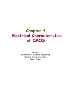
www.ee.ncu.edu.twA simplified linear model of MOS is useful at the logic level design RC model of an NMOS The drain-source resistance at any point on the current curve as shown below Drain-Source MOS Resistance S D C s C D R n G S D G V ds I ds a b c. Advanced Reliable Systems (ARES) Lab. Jin-Fu Li, EE, NCU 5