Pcb design guidelines for qfn and
Found 5 free book(s)
AN18.15 PCB Design Guidelines for QFN and DQFN Packages
ww1.microchip.com2014 Microchip Technology Inc. DS00001843A-page 3 AN18.15 Routing Hazards QFN PACKAGES Avoid routing between the flag and the pads of a QFN device, as shown in Figure 4 below.
Soldering Guidelines for Mounting Bottom-terminated …
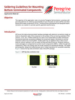
www.psemi.comApplication Note 62 Soldering Guidelines for BTCs DOC-78164-1 – (10/2016) Page 5 www.psemi.com Termination Pad Stencil Design The stencil aperture for the terminal fingers is typically designed to match the PCB/substrate

Printing and Assembly Challenges for Quad Flat No-lead ...
www.photostencil.comPRINTING AND ASSEMBLY CHALLENGES FOR QUAD FLAT NO-LEAD (QFN) PACKAGES With proper stencil design, stencil technology selection,

QFN Layout Guidelines - Texas Instruments
www.ti.comwww .ti.com 2.1.2 Thermal Vias Thermal Via Web or Spoke Via NOT Recommended Solid Via Recommended Exposed Copper! 0,05 mm Around Via Board Layout Inner or bottom layer copper planes also can be connected to thermal pad using vias and should be made

Manufacturing and Reliability Challenges With QFN (Quad ...
asq.org1 Manufacturing and Reliability Challenges With QFN (Quad Flat No Leads) Cheryl Tulkoff ASQ Reliability Society Webinar March 10, 2011