Pnp Silicon
Found 8 free book(s)
BC556B, BC557A, B, C, BC558B - Amplifier Transistors PNP ...
www.onsemi.comPNP Silicon Features • Pb−Free Packages are Available* MAXIMUM RATINGS Rating Symbol Value Unit Collector - Emitter Voltage BC556 BC557 BC558 VCEO −65 −45 −30 Vdc Collector - Base Voltage BC556 BC557 BC558 VCBO −80 −50 −30 Vdc Emitter - Base Voltage VEBO −5.0 Vdc Collector Current − Continuous Collector Current − Peak IC ...
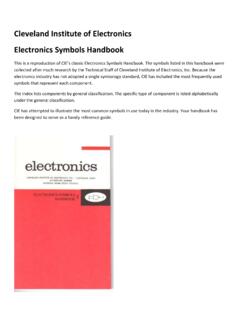
Cleveland Institute of Electronics Electronics Symbols ...
www.cie-wc.eduscr (silicon controlled rectifier anode gate anode scs (silicon cathode cathode gate controlled switch triac gate transistors igfet, mosfet , igfet , mosfet channel channel . ... pnp transistor pnpn transistor two gate nosfet emitter unijunction transistor shielded wire , single conductor wire shielded between two points

14. Transistor Characteristics Lab
www.hunter.cuny.edupnp Transistor When the two n regions are next to each other (as below) then one has a pnp transistor. ... This voltage drop is a constant 0.7 for a silicon based junction. (If less common germanium is used instead of silicon, the voltage drop is 0.3 volts) Conservation of potential yields Vcb +Vbe = Vce (4)
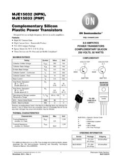
MJE15032 - Complementary Silicon Plastic Power Transistors
www.onsemi.comMJE15033 (PNP) Complementary Silicon Plastic Power Transistors Designed for use as high−frequency drivers in audio amplifiers. Features • High DC Current Gain • High Current Gain − Bandwidth Product • TO−220 Compact Package • Epoxy Meets UL 94 V−0 @ 0.125 in • These Devices are Pb−Free and are RoHS Compliant* MAXIMUM RATINGS

Insulated Gate Bipolar Transistor (IGBT) Basics
www.ixys.comevident that the silicon cross-section of an IGBT is almost identical to that of a vertical Power MOSFET except for the P+ injecting layer. It shares similar MOS gate structure and P wells with N+ source regions. The N+ layer at the top is the source or emitter and the P+ layer at the bottom is the drain or collector. It is also feasible to ...

Failure Mechanisms of Insulated Gate Bipolar Transistors ...
www.nrel.govburn-out (Silicon die) High electric field, overvoltage, ionizing radiation Latch-up (V CE(ON)) Open Circuit (Bond Wire) High temperature, high current densities Bond Wire Cracking, Lift Off (V CE(ON)) Open Circuit (Die Attach) CE(ON) Voiding, Delamination of Die Attach (V ) High temperature, high current densities
Chapter 1 Power Electronic Devices (Part I)
pdfs.semanticscholar.orgAnother name: SCR—silicon controlled rectifier Thyristor Opened the power electronics era – 1956, invention, Bell Laboratories – 1957, development of the 1st product, GE – 1958, 1st commercialized product, GE – Thyristor replaced vacuum devices in almost every power processing area. Still in use in high power situation. Thyristor till ...

T B S U N I F Y P R O 5 G 8 ( H V ) V i d e o T r a n s m ...
www.team-blacksheep.comExample: PNP25/PNP50/PNP PRO) 6V to 28V (2S - 6S) VBat, peak max 31V Please connect directly to battery voltage! Power O u tp u t None 5V for Camera @ 0.5A max. Ex tra f ea tu res : CleanSwipe PitMode R em ote s of twa re p rotocol SmartAudio V2.0 LITE ( r equires 3.3V level and soft- or hardware pull low ) ,