Power Gan
Found 8 free book(s)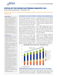
STATUS OF THE POWER ELECTRONICS INDUSTRY 2021
s3.i-micronews.comIncluded:power silicon (excluding power ICs), p ower SiC and power GaN CAGR 20-26:Discrete 6.9% 2020 $17.5B 2026 $26.2B Module 37% Discrete Module 63% 30% 70% 2000 2020 8-inch 12-inch 2025 Race for 12-inch capacity to fulfill demand from different segments Infineon was the first to produce IGBT in 12-inch wafers

GaN Power HEMT Tutorial: GaN Basics
iganpower.com1,Kevin J. Chen, Understanding the Dynamic Behavior in GaN-on-Si Power Devices and IC’s, Integrated Power Conversion and Power Management, 2018 2,Greco, G., Iucolano, F., & Roccaforte, F. Review of technology for normally-off HEMTs with p-GaN gate. Materials Science in Semiconductor Processing GIT p-GaN p-GaN

Company Presentation - STMicroelectronics
www.st.comBCD, VIPower*, SiC, GaN and power MOSFET. Unique expertise in RF and analog design using advanced technologies, such as RFSOI, BiCMOS and millimeter wave. Digital ASICs. Analog & RF ASICs. Power ASICs. Proprietary micromachining process, deep expertise in MEMS integration. Custom imaging solutions and premium foundry services. MEMS and imaging ...
7. Kinetic Energy and Work Kinetic Energy
www.asc.ohio-state.eduPower: Consider a box being dragged up a ramp. The work done is: W = F cos qd Whether the box is dragged quickly or slowly up the ramp, the work done is the same. However, doing the work quickly requires more effort. The quickness of doing the work is characterized using the concept of Power: Power is the work done per unit time.
Fundamentals of Gallium Nitride Power Transistors
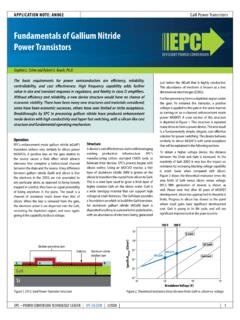
epc-co.comEPC’s enhancement mode gallium nitride (eGaN®) transistors behave very similarly to silicon power MOSFETs. A positive bias on the gate relative to the source causes a field effect which attracts electrons that complete a bidirectional channel between the drain and the source. A key difference between gallium nitride (GaN) and silicon is that
Gallium Nitride (GaN) versus Silicon Carbide (SiC)
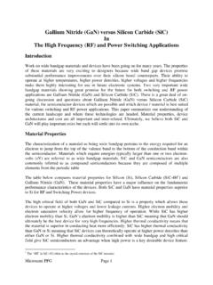
www.richardsonrfpd.comGallium Nitride (GaN). These material properties have a major influence on the fundamental performance characteristics of the devices. Both SiC and GaN have material properties superior to Si for RF and Switching Power devices. The high critical field of both GaN and SiC compared to Si is a property which allows these
The Faerie Queene - Scholars' Bank Home
scholarsbank.uoregon.eduNot perceable with power of any starre: And all within were pathes and alleies wide, With footing worne, and leading inward farre: Faire harbour that them seemes; so in they entred arre. And foorth they passe, with pleasure forward led, Ioying to heare the birdes sweete harmony, Which therein shrouded from the tempest dred,
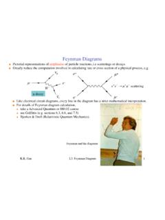
Feynman Diagrams - College of Arts and Sciences
www.asc.ohio-state.eduK.K. Gan L3: Feynman Diagram 1 Pictorial representations of amplitudes of particle reactions, i.e scatterings or decays. Greatly reduce the computation involved in calculating rate or cross section of a physical process, e.g. Like electrical circuit diagrams, every line in the diagram has a strict mathematical interpretation.