Semiconductor Switch
Found 12 free book(s)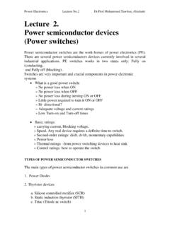
Lecture 2. Power semiconductor devices (Power switches)
www.philadelphia.edu.joAny real device requires a definite time to switch. » Second-order ratings: di/dt, dv/dt, momentary capabilities. » Power loss » Thermal ratings –from power switching devices to heat sink » Control ratings: how to operate the switch TYPES OF POWER SEMICONDUCTOR SWITCHES The main types of power semiconductor switches in common use are 1.
Technical Explanation for Basic Switches - Omron
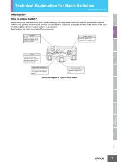
www.ia.omron.comSwitch with Contacts: A type of switch that achieves the switching function through the mechanical switching of contacts. Use as opposed to a semiconductor switch with switch characteristics. Contact Form: The structure of the electrical I/O circuits of contacts used according to the type of application. (Refer to Contact Form

Power Semiconductor Devices - Pearson
www.pearsonhighered.comPower semiconductor devices constitute the heart of modern power electronic apparatus. ... As a result, the diode has a lower conduction drop (typically 0.5 V) and faster switch-ing time, but the limitations are a lower blocking voltage (typically up to 200 V) and higher leak-age current. For example, the International Rectifier Schottky diode ...
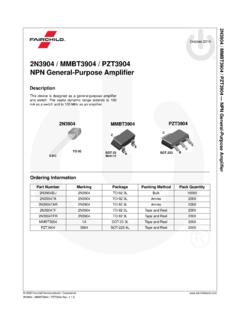
2N3904 MMBT3904 PZT3904 - NPN General-Purpose Amplifier
www.mouser.comJul 14, 2008 · and switch. The useful dynamic range extends to 100 mA as a switch and to 100 MHz as an amplifier. ... FAIRCHILD SEMICONDUCTOR RESERVES THE RIGHT TO MAKE CHANGES WITHOUT FURTHER NOTICE TO ANY PRODUCTS HEREIN TO IMPROVE RELIABILITY, FUNCTION, OR DESIGN. TO OBTAIN THE LATEST, MOST UP-TO-DATE …
Basic Electronics - New York University
engineering.nyu.edu• A three lead semiconductor device that acts as: – an electrically controlled switch, or – a current amplifier. • Transistor is analogous to a faucet. – Turning faucet’s control knob alters the flow rate of water coming out from the faucet. – A small voltage/current applied at transistor’s control lead controls a …
Edwards iH Dry Pumping Systems, iH80, iH600, iH1000
www.idealvac.comSafety Guidelines for Semiconductor Manufacturing Equipment. Non Electrical Equipment for Potentially Explosive Atmospheres. Low Voltage Directive. ... 6.18 Disconnect box and photohelic switch/gauge (accessories) 6-19 6.18.1 Introduction 6-20 6.18.2 Fault finding6-20 6.18.3 Fuse replacement 6-20 7 STORAGE AND DISPOSAL 7-1 7.1 Storage 7-1

Automotive Gateway: A Key Component to Securing the ...
www.nxp.comFlexRay Switch Interface Ethernet PHY Ethernet Network(s) FlexRay Network Gateway LIN Processor Interface Power Management ... NXP Semiconductor Hong Kong Ltd. Technical Information Center 2 Dai King Street Tai Po Industrial Estate Tai Po, N.T., Hong Kong +800 2666 8080 support.asia@nxp.com

NCP1654 - ON Semiconductor
www.onsemi.comthe power switch conduction time (PWM) in a fixed frequency mode and in dependence on the instantaneous coil current. Housed in a SO8 package, the circuit minimizes the number of external components and drastically simplifies the PFC implementation. It also integrates high safety protection features that

AN-1484Designing A SEPIC Converter - Semiconductor …
www.ti.comIn a SEPIC converter, when the power switch Q1 is turned on, the inductor is charging and the output current is supplied by the output capacitor. As a result, the output capacitor sees large ripple currents. Thus the selected output capacitor must be capable of handling the maximum RMS current. The RMS current in the output capacitor is: (14 ...
Basic Electronics
engineering.nyu.edu• A three lead semiconductor device that acts as: – an electrically controlled switch, or – a current amplifier. • Transistor is analogous to a faucet. – Turning faucet’s control knob alters the flow rate of water coming out from the faucet. – A small voltage/current applied at transistor’s control lead controls a larger current ...
Chapter 7 Gate Drive circuit Design - Fuji Electric
www.fujielectric.coma drive circuit has a forward bias power supply alternately switching back and forth using switch S; 1; and S; 2. During this switching, the current used to charge and discharge the gate, is the driven current. In Fig. 7-4, the area showing the current waveform (the hatched area) is equivalent to the gate charge

2N3904DB - NPN General - Purpose Amplifie - ON …
www.onsemi.com2N3904 www.onsemi.com 2 ELECTRICAL CHARACTERISTICS (Values are at TA = 25°C unless otherwise noted.) Symbol Parametr Conditions Min Max Unit OFF CHARACTERISTICS V(BR)CEO Collector−Emitter Breakdown Voltage IC = 1.0 mA, IB = 0 40 − V V(BR)CBO Collector−Base Breakdown Voltage IC = 10 A, IE = 0 60 − V V(BR)EBO Emitter−Base …