Silicon Power Semiconductor Device
Found 9 free book(s)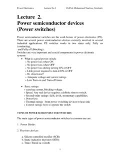
Lecture 2. Power semiconductor devices (Power switches)
www.philadelphia.edu.jopower supplies. 2.2 Thyristors ( Silicon Controlled Rectifiers “SCRs”) The thyristor ,it is also called silicon controlled rectifier (SCR), is a four-layer, three terminal switching semiconductor device, with each layer consisting of an alternately N or P-type material, for example N-P-N-P. The main terminals,
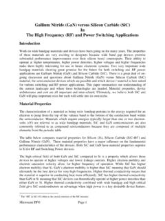
Gallium Nitride (GaN) versus Silicon Carbide (SiC)
www.richardsonrfpd.comapplications are Gallium Nitride (GaN) and Silicon Carbide (SiC). There is a great deal of on-going discussion and questions about Gallium Nitride (GaN) versus Silicon Carbide (SiC) material, the semiconductor devices which are possible and which device / material is best suited for various switching and RF power applications.
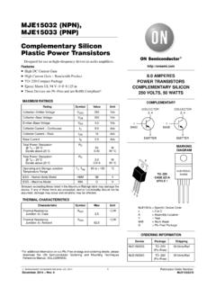
Complementary Silicon Plastic Power ... - ON Semiconductor
www.onsemi.comTotal Power Dissipation @ TA = 25 C Derate above 25 C PD 2.0 0.016 W W/ C Operating and Storage Junction Temperature Range TJ, Tstg –65 to +150 C ESD − Human Body Model HBM 3B V ESD − Machine Model MM C V Stresses exceeding those listed in the Maximum Ratings table may damage the device. If any of these limits are exceeded, device ...
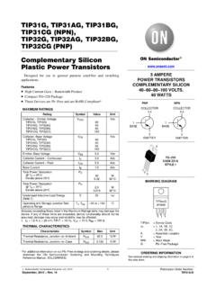
Complementary Silicon Plastic Power ... - ON Semiconductor
www.onsemi.comTotal Power Dissipation @ TA = 25°C Derate above 25°C PD 2.0 0.016 W W/°C Unclamped Inductive Load Energy (Note 1) E 32 mJ Operating and Storage Junction Tem-perature Range TJ, Tstg –65 to +150 °C Stresses exceeding those listed in the Maximum Ratings table may damage the device. If any of these limits are exceeded, device functionality ...
Power Semiconductor Reliability Handbook
www.aosmd.comPower Semiconductor Reliability Handbook ... There are certain wear-out mechanisms in a semiconductor device, such as electromigration, hot carrier degradation of a ... time, if the design rules given by a reputable silicon foundry are …
MOSFET Device Physics and Operation
homepages.rpi.educase of a p-type substrate (n-channel device) or holes in the case of an n-type substrate (p-channel device), induced in the semiconductor at the silicon-insulator interface by the voltage applied to the gate electrode. The electrons enter and exit the channel at n+ source and drain contacts in the case of an n-channel MOSFET, and at p+ ...

Wide Bandgap Semiconductors: Pursuing the Promise
www1.eere.energy.govWide bandgap (WBG) semiconductor . materials allow power electronic components to be smaller, faster, more reliable, and more efficient than their silicon (Si)-based counterparts. These capabilities make it possible to reduce weight, volume, and life-cycle costs in a wide range of power applications. Harnessing these capabilities can lead

Introduction to Semiconductor Technology ...
www.st.comINTRODUCTION TO SEMICONDUCTOR TECHNOLOGY by Microcontroller Division Applications INTRODUCTION An integrated circuit is a small but sophisticated device implementing several electronic func-tions. It is made up of two major parts: a tiny and very fragile silicon chip (die) and a package

SEMICONDUCTOR DEVICE PHYSICS AND DESIGN
seklad69associates.comSemiconductor Device Physics and Design UMESH K. MISHRA University of California, Santa Barbara, CA, USA and JASPRIT SINGH The University of Michigan, Ann Arbor, MI, USA