Silicon Transistors
Found 10 free book(s)
TIP110, TIP111, TIP112 (NPN); TIP115, TIP116, TIP117 (PNP ...
www.onsemi.comComplementary Silicon Transistors Designed for general−purpose amplifier and low−speed switching applications. Features • High DC Current Gain − hFE = 2500 (Typ) @ IC = 1.0 Adc • Collector−Emitter Sustaining Voltage − @ 30 mAdc VCEO(sus) = 60 Vdc (Min) − TIP110, TIP115 = 80 Vdc (Min) − TIP111, TIP116 = 100 Vdc (Min) − TIP112 ...

Diodes and Transistors
inst.eecs.berkeley.eduDiodes and Transistors 1. Introduction So far in EE100 you have seen analog circuits. You started with simple resistive circuits, ... Silicon doped with acceptors is also called a p-type semiconductor because of the abundance of holes. Figure 3. Silicon doped with boron. The movement of an electron to the left is equivalent to a hole
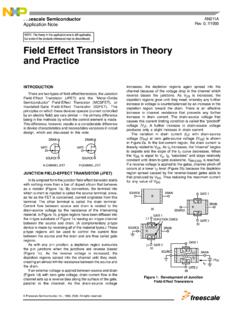
Field Effect Transistors in Theory and Practice ...
www.nxp.comField Effect Transistors in Theory and Practice INTRODUCTION There are two types of field-effect transistors, theJunction Field-Effect Transistor (JFET) and the “Metal-Oxide ... Silicon nitride is impervious to sodium ions and thus is used to …

Experiment 6 Transistors as amplifiers and switches
www.sophphx.caltech.eduTransistors as amplifiers and switches Our final topic of the term is an introduction to the transistor as a discrete circuit element. Since an integrated circuit is constructed primarily from dozens to even millions of transistors formed from a single, thin silicon crystal, it might be interesting and instructive to
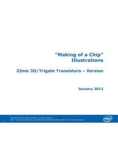
“Making of a Chip”
download.intel.comthe silicon. This alters the conductive properties of the silicon (making it conductive or insulating, depending on the type of ion used) in selected locations. Here we show the creation of wells, which are regions within which transistors will be formed. Removing Photoresist– scale: wafer level (~300mm / 12 inch)

BF245A; BF245B; BF245C N-channel silicon field-effect ...
www.nxp.comN-channel silicon field-effect transistors BF245A; BF245B; BF245C LIMITING VALUES In accordance with the Absolute Maximum Rating System (IEC 134). Note 1. Device mounted on a printed-circuit board, minimum lead length 3 mm, mounting pad for drain lead minimum 10 mm 10 mm. THERMAL CHARACTERISTICS STATIC CHARACTERISTICS

MPS2222, MPS2222A General Purpose Transistors
www.farnell.comTransistors NPN Silicon Features • Pb−Free Packages are Available* MAXIMUM RATINGS Rating Symbol Value Unit Collector−Emitter Voltage MPS2222 MPS2222A VCEO 30 40 Vdc Collector−Base Voltage MPS2222 MPS2222A VCBO 60 75 Vdc Emitter−Base Voltage MPS2222 MPS2222A VEBO 5.0 6.0 Vdc Collector Current − Continuous IC 600 mAdc Total Device ...

2N4401 General Purpose Transistors
www.farnell.comTransistors NPN Silicon Features • Pb−Free Packages are Available* MAXIMUM RATINGS Rating Symbol Value Unit Collector − Emitter Voltage VCEO 40 Vdc Collector − Base Voltage VCBO 60 Vdc Emitter − Base Voltage VEBO 6.0 Vdc Collector Current − Continuous IC 600 mAdc Total Device Dissipation @ TA = 25°C Derate above 25°C PD 625 5.0 mW ...

Lecture 3: Diodes and Transistors - MIT OpenCourseWare
ocw.mit.eduSep 17, 2007 · Silicon Diode • 0.7V turn-on • Important specs: – Maximum forward current – Reverse leakage current – Reverse breakdown voltage • Typical parts: Part # I F, max I R V R, max Cost 1N914 200mA 25nA at 20V 100 50V ~$0.007 1N4001 1A 5µA at 50V ~$0.02

ON Semiconductor Is Now
www.onsemi.comNPN Epitaxial Silicon Transistor Absolute Maximum Ratings Ta=25°C unless otherwise noted Electrical Characteristics Ta=25°C unless otherwise noted * Pulse Test: Pulse Width≤300µs, Duty Cycle≤2% Symbol Parameter Value Units VCBO Collector-Base Voltage 60 V VCEO Collector-Emitter Voltage 30 V VEBO Emitter-Base Voltage 5 V IC Collector ...