Stray Dc Voltage
Found 9 free book(s)
IEC 60364-6: Low voltage electrical installations – Part 6 ...
www.emo.org.trThe stray capacitance between active conductors and ground slows the voltage change, hence test voltage time rises. Test instrument shall generate voltage for a sufficient time for the transients to die ... Nominal circuit voltage DC test voltage [V] Insulation resistance [MΩ] SELV and PELV 250 ≥ 0,5 Up to and including 500 V, including FELV ...
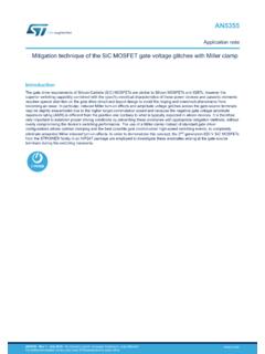
Mitigation technique of the SiC MOSFET gate voltage ...
www.st.comInductive parasitic turn-on can be also generated during turning off of the load current when a voltage is induced across the emitter stray inductance. In this condition, the decay of the current induces a voltage on source stray inductance that shifts the source potential to the negative level. The inductive parasitic turn-on, however, can be
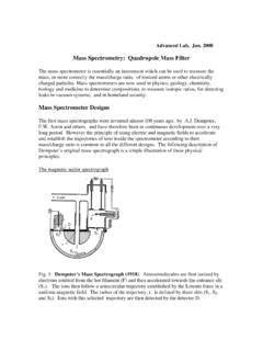
Mass Spectrometry: Quadrupole Mass Filter Mass ...
instructor.physics.lsa.umich.eduof stray magnetic fields can affect other instruments that may be used in conjunction with a mass spectrometer, for example, electron energy analyzers. ... (U+Vcos(ωt)), where U is a dc voltage and Vcos(ωt) is an ac voltage. The applied voltages affect the trajectory of ions traveling down the flight path centered between the four rods. For ...
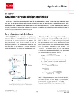
Snubber circuit design methods - Rohm
fscdn.rohm.comwaveform of the surge voltage when LS turns off is shown in Figure 4. Figure 3 C Snubber Surge voltage is reduced by more than 50V (reaching 901V) and ringing frequency increases to 44.6MHz. It is because C SNB is placed close to the switches and as a result, the stray inductances (L SNB) involved in the switching path is reduced. In this case ...

MULTISTAGE AMPLIFIER - MIT
web.mit.eduExample, CD-CC voltage buffer: • Advantages – No capacitors needed – compact • Disadvantages – Bias point shared:constrains designs. – Bias shifts from stage to stage and can stray too far from center of range – Generally requires level shifting to bring signal back to center of range. 4.7 V 5.0 V 2.5 V 3.2 V Assumes V BE = 0.7 V ...

2. Operational Amplifiers
www.cs.tut.fiOutput Voltage Swing Output Current Limits. Figure 2.28 . For a real op amp, clipping occurs if the output voltage reaches certain limits. For µA741: If the supply voltages are +15V and –15V the amplitude of the output voltage without clipping is 14V typically (guaranteed is 12V). The maximum that an Op Amp can supply to a load is restricted.
Low-power dual operational amplifiers
www.st.comSupply voltage ±16 or 32 V i Input voltage -0.3 to 32 V V id Differential input voltage ±32 Output short-circuit duration (1) Infinite I in Input current (2) 5 mA in DC or 50 mA in AC (duty cycle = 10 %, T = 1 s) mA T oper Operating free-air temperature range -55 to 125 -40 to 105 0 to 70 T stg Storage temperature range -65 to 150 °C T j
Class D Amplifier Design Basics II
www.irf.com6. Power supply voltage fluctuations due to its finite output impedance and reactive power flowing through the DC bus 7. Non-linearity in the output LPF. Note that 0.01% of non-linearity corresponds to10mV out of 100V DC bus, or 0.25ns in 400kHz! F/B
LECTURE 14 THE MOS SWITCH AND MOS DIODE
aicdesign.orgCurrent-Voltage Characteristics of a NMOS Switch The following simulated output characteristics correspond to triode operation of the MOSFET. SPICE Input File: MOS Switch On Characteristics M1 1 2 0 3 MNMOS W=1U L=1U .MODEL MNMOS NMOS VTO=0.7, KP=110U, +LAMBDA=0.04, GAMMA=0.4 PHI=0.7 VDS 1 0 DC 0.0 VGS 2 0 DC 0.0 VBS 3 0 DC -5.0