The Output Impedance
Found 6 free book(s)
Differential Impedance …finally made simple
ewh.ieee.orgTDR: 400 mV output, unloaded 50W output impedance V measured (DUT) Device Under Test 3 different line width microstrips, each 9 inches long 50W cable TDR response 50 mV/div 500 psec/div--400mV--300mV--200mV--100mV--0mv Eric Bogatin 2000 Slide -31 www.BogatinEnterprises.com MYTHS
Low-noise JFET quad operational amplifier - …
www.st.com• Output short-circuit protection • High input impedance JFET input stage • Low harmonic distortion: 0.01% (typical) • Internal frequency compensation • Latch up free operation • High slew rate: 16 V/µs (typical) Related products • See TL071 for single version

4 x 50 W MOSFET quad bridge power amplifier
www.st.comVOS Output offset voltage Play mode / Mute mode ±50 mV dVOS During mute ON/OFF output offset voltage ITU R-ARM weighted see Figure 20-10 +10 mV During Standby ON/OFF output offset voltage-10 +10 mV Gv Voltage gain 25 26 27 dB dGv Channel gain unbalance ±1 dB Po Output power VS = 13.2 V; THD = 10 % VS = 13.2 V; THD = 1 % VS = 14.4 V; THD = 10 %
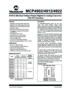
MCP4902/4912/4922 Data Sheet - Microchip Technology
ww1.microchip.comchannel are turned off for power savings and the output amplifier is configured to present a known high resistance output load (500 k typical . The devices include double-buffered registers, allowing synchronous updates of two DAC outputs, using the LDAC pin. These devices also incorporate a Power-on Reset (POR) circuit to ensure reliable power-
Adjustable Output, Positive D2PAK 3 D2T SUFFIX CASE 936
www.onsemi.comLM317, NCV317 www.onsemi.com 2 MAXIMUM RATINGS Rating Symbol Value Unit Input−Output Voltage Differential VI−VO −0.3 to 40 Vdc Power Dissipation Case 221A TA = +25°C PD Internally Limited W Thermal Resistance, Junction−to−Ambient JA 65 °C/W Thermal Resistance, Junction−to−Case JC 5.0 °C/W Case 936 (D2PAK−3) TA = +25°C PD Internally …
Low Cost Low Power Instrumentation Amplifier AD620
www.analog.comOutput Offset, V OSO V S = ±15 V 400 1000 200 500 400 1000 μV V S = ± 5 V 1500 750 1500 μV Overtemperature V S = ±5 V to ± 15 V 2000 1000 2000 μV Average TC V S = ±5 V to ± 15 V 5.0 15 2.5 7.0 5.0 15 μV/°C Offset Referred to the