Search results with tag "Band gap"

The Use of UV-visible Spectroscopy to Measure the Band Gap ...
mmrc.caltech.eduelectronic band gap, which is defined as the energy difference between the valence band minimum (VBM) and the conduction band maximum (CBM); however, it is often approximated as such because there are few convenient methods for measuring the electronic band gap. Exciton binding energies, d-d transitions, phonon absorption and

Metal/Semiconductor Ohmic Contacts - Stanford University
web.stanford.eduBandgap Engineering Contact resistance depends on barrier height. It is possible to use a lower bandgap material in the source/drain such as Si1-xGex. Band gap of Si1-xGex reduces as compared to Si as Ge fraction increases. • Si1-xGex S/D & germanosilicide contact − Assuming metal Fermi level is pinned near midgap

Determination of the Band-Gap of a Semiconductor ...
www.ijsr.netsilicon photonics. They calculate the energy band variation as a function of strain and inferred that the crossover from indirect to direct band gap occurs for a tensile in-plane strain of 1.9%. The effective masses of density of states are deduced from the calculated conduction and valence band density of states.
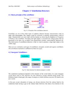
Chapter 4 Scintillation Detectors - McMaster Faculty of ...
www.science.mcmaster.caFig. 4.2. Band structure for electron energies in solids. The scintillation mechanism depends on the structure of the crystal lattice. In a pure inorganic crystal lattice such as NaI, electrons are only allowed to occupy selected energy bands. The forbidden band or band gap is the range of energies in which electrons can never be found in the

TMP35/TMP36/TMP37 Low Voltage Temperature Sensors …
www.arduino.ccheart of the temperature sensor is a band gap core, which is comprised of transistors Q1 and Q2, biased by Q3 to approxi-mately 8 µA. The band gap core operates both Q1 and Q2 at the same collector current level; however, since the emitter area of Q1 is 10 times that of Q2, Q1’s V BE and Q2’s V BE are not equal by the following ...