Search results with tag "Switch node"

Minimizing Ringing at the Switch Node of a Boost …
www.ti.comwww .ti.com Description of the Problem Figure 2. Ringing at Switch Node of Boost Converter Figure 2 shows a scope plot of the switch node of a boost …
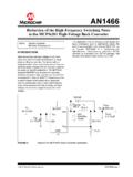
Reduction of the High-Frequency Switching Noise in the ...
ww1.microchip.comNov 29, 2012 · for the main switch, as described above. The input source should be decoupled to GND with a 4.7 µF-20 µF capacitor, depending on the impedance of the source and the output current. The input capaci-tor provides current for the switch node and a …
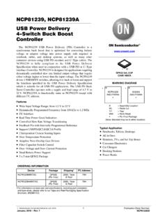
NCP81239DB - USB Power Delivery 4-Switch Buck Boost …
www.onsemi.com31 VSW1 Switch Node. VSW1 pin swings from a diode voltage drop below ground up to V1. 32 BST1 Driver Supply. The BST1 pin swings from a diode voltage below VDRV up to a diode voltage below V1 + VDRV. Place a 0.1 F capacitor from this pin to VSW1. 33 THPAD Center Thermal Pad. Connect to AGND externally. Table 2.

Common Mistakes in DC/DC Converters and How to Fix …
www.ti.commode are shown in Figure 1. A simplified switch node voltage (V SW) and inductor current waveform are shown in Figure 2. While other converter topologies, like the boost converter, buck-boost converter, series capacitor buck converter [1][2] and many others may also be used, this discussion focuses on the buck converter for simplicity.

CHOOSING A THEME FOR YOUR MEETING - Get Switchedon
getswitchedon.comthroughout the year to remind our people to stay switched on and to focus on what they can do to make a difference in their own results. Chip brought great energy, a solid message and he engaged the audience through collaboration and discussions. The …
Switched-On
glnmedia.s3.amazonaws.comWelcome to Switched-On Schoolhouse® This guide walks you through how to install Switched-On Schoolhouse (SOS) and do the basic setup necessary for your student(s) to begin their schoolwork.