Search results with tag "Mc34063"

Application of the MC34063 Switching Regulator (Rev. B
www.ti.comMC34063 Description The output switch is an NPN Darlington transistor. The collector of the output transistor is tied to pin 1, and the emitter is tied to pin 2. This allows the designer to use the MC34063 in buck, boost, or inverter configurations. The maximum collector-emitter saturation voltage at 1.5 A (peak) is 1.3 V, and the
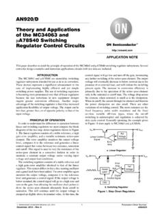
AN920/D Theory and Applications of the MC34063 and …
www.onsemi.comThe MC34063 series is a monolithic control circuit containing all the active functions required for dc to dc converters. This device contains an internal temperature compensated reference, comparator, controlled duty cycle oscillator with an active peak current limit circuit, driver, and a high current output switch. This series was specifically
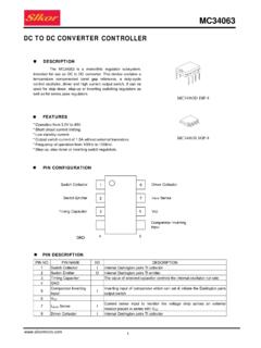
DC TO DC CONVERTER CONTROLLER - szlcsc.com
atta.szlcsc.comThe MC34063 is a monolithic regulator subsystem, intended for use as DC to DC converter. This device contains a temperature compensated band gap reference, a duty-cycle control oscillator, driver and high current output switch. It can be used for step down, step-up or inverting switching regulators as well as for series pass regulators. FEATURES
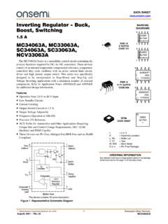
MC34063A - Inverting Regulator - Buck, Boost, Switching 1.5 A
www.onsemi.comMC33063, MC34063 MC33063V, NCV33063 Regline − − 1.4 1.4 5.0 6.0 mV Input Bias Current (Vin = 0 V) IIB − −20 −400 nA TOTAL DEVICE Supply Current (VCC = 5.0 V to 40 V, CT = 1.0 nF, Pin 7 = VCC, VPin 5 > Vth, Pin 2 = GND, remaining pins open) ICC − − 4.0 mA