Search results with tag "Output stage"
Burning Amp Number Three - FIRST WATT
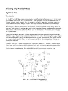
www.firstwatt.comThe official BA #1 single-ended output stage now looks like this: And the official BA #2 push-pull output stage looks like this: Both of these circuits now include the necessary components to bias the output stages.
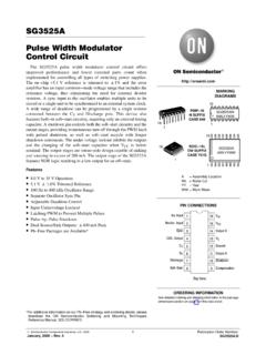
SG3525A - Pulse Width Modulator Control Circuit
www.onsemi.comnominal. The output stages are totem−pole design capable of sinking and sourcing in excess of 200 mA. The output stage of the SG3525A features NOR logic resulting in a low output for an off−state. Features •8.0 V to 35 V Operation •5.1 V 1.0% Trimmed Reference •100 Hz to 400 kHz Oscillator Range •Separate Oscillator Sync Pin
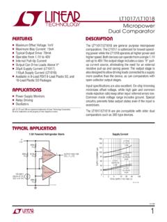
LT1017/LT1018 - Micropower Dual Comparator
www.analog.comThe output stage includes a class “B” pull-up current source, eliminating the need for an external resistive pull-up and saving power. The output stage is also designed to allow driving loads connected to a supply more positive than the device, as can comparators with

MT-041: Op Amp Input and Output Common-Mode and ...
www.analog.comuse a separate output stage (within the feedback loop) to minimize self-heating of the precision op amp. This added amplifier is often called a buffer, since it typically will have a voltage gain = 1. Page 3 of 4 . Page 4 of 4 MT-041 There are some op amps that are designed to give large output currents. An example is the

MLX90316 Rotary Position Sensor IC - Melexis
www.melexis.comOutput Stage 12 bit Analog 12 bit PWM SPI G EEPROM DSP RAM µC ROM - Firmware V SS V OUT1 MOSI/MISO OUT2 SCLK ... Active Diagnostic Output Level Diag_lo Pull-down load R. L. Pull-up load R. L. 1 1.5 %V. DD %V. DD. Diag_hi . Pull-down load R. L & < MLX90316 Rotary Position Sensor IC Datasheet (& ) & & .
MCP2561/2 Data Sheet - Microchip Technology
ww1.microchip.comtransmitter output stage during such a Fault condition. ... CANH and CANL output drivers in order to prevent the corruption of data on the CAN bus. The drivers will ... T XD is connected to an internal pull-up resistor (nominal 33 k ) to V DD or V IO, in …

MCP2551 High-Speed CAN Transceiver
ww1.microchip.comNov 07, 2016 · the RXD output pin correspond to the Dominant and Recessive states of the CAN bus, respectively. 1.3 Internal Protection CANH and CANL are protected against battery short circuits and electrical transients that can occur on the CAN bus. This feature prevents destruction of the transmitter output stage during such a fault condition.

Pure Class A operation delivers quality power: 45 …
www.accuphase.comPure Class A operation delivers quality power: 45 watts x 2 into 8 ohms Power MOS-FET output stage features 6-parallel push-pull configuration