Search results with tag "Layout guidelines"

QFN Layout Guidelines - Texas Instruments
www.ti.com6 QFN Layout Guidelines SLOA122– July 2006 Submit Documentation Feedback. IMPORTANT NOTICE Texas Instruments Incorporated and its subsidiaries (TI) reserve the right to make corrections, modifications, enhancements, improvements, and other changes to its products and services at any time and to discontinue
DDR2, DDR3, and DDR4 SDRAM Board Design Guidelines 4
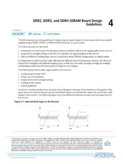
www.intel.co.jp• Layout guidelines As memory interface performance increases, board designers must pay closer attention to the quality of the ... Controllers must compensate for this skew by adjusting the timing per byte lane. During a write, DQS groups launch at separate times to coincide with a clock arriving at components on ... power-up or when the DDR3 ...
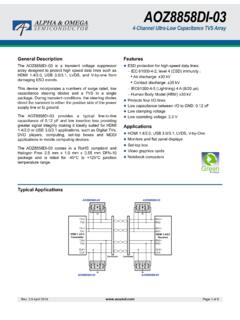
AOZ8858DI-03 - Alpha and Omega Semiconductor
www.aosmd.comAOZ8858DI-03 Rev. 2.0 April 2017 www.aosmd.com Page 5 of 8 High Speed PCB Layout Guidelines Printed circuit board layout is the key to achieving the highest level of surge immunity on power and data lines.