Transcription of 7 A VI Chip EMI Filter SiP - Vicor Corporation
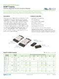
1 Quiet-Power . QPI-12. 7 a vi chip EMI Filter SiP . Product Description Features The QPI-12 EMI lter is speci cally designed to attenuate 45 dB CM attenuation at 1 MHz (50 ). conducted common-mode (CM) and di erential-mode (DM) 75 dB DM attenuation at 1 MHz (50 ). noise of Vicor 's VI chip products, such as the PRM , VTM 80 Vdc (max input). and BCM converters, to comply with the CISPR22 standard 100 Vdc surge 100 ms requirements for conducted noise measurements. The lter is designed to operate up to 80 Vdc, 100 Vdc surge, and supports 1,500 Vdc hipot hold off to shield plane 7 A loads up to 85 C (TA) without de-rating. 7 A rating Designed for the telecom bus range, the VI chip EMI lter x x mm, lidded SiP (System-in-Package). supports the PICMG speci cation for ltering system x x mm, open-frame boards to the EN55022 Class B limits.
2 Low profile LGA package -40 to +125 C PCB temperature (see Figure 6). Efficiency >99%. T V Certified Applications Figure 1 QPI-12LZ (~1/2 in2 area) VI chip input EMI Filter Telecom and ATCA boards Typical Applications BUS+. CIN L. BUS+ QPI+ IN+ OUT+ IN+ OUT+. LOAD. CB1 + +. PRM VTM Optional Chassis Connection BUS- QPI- IN- OUT- IN- OUT- Shield BUS- CY1 CY2. CY3 CY4. Chassis/Shield Shield Plane Figure 2 Typical QPI-12 application schematic with Vicor 's PRM and VTM modules. [a]. BUS+. CIN. BUS+ QPI+ IN+ OUT+. LOAD. CB1 + +. BCM Optional Chassis Connection BUS- QPI- IN- OUT- Shield BUS- CY1 CY2. CY3 CY4. Chassis/Shield Shield Plane Figure 3 Typical QPI-12 application schematic with Vicor 's BCM module. [a]. [a] CB1 capacitor, referenced in all schematics, is a 47 uF electrolytic; United Chemi-Con EMVE101 ARA470 MKE0S or equivalent.
3 CY1 to CY4, referenced in all schematics, are nF hi-voltage safety capacitors; Vishay VY1472M63Y5UQ63V0 or equivalent. Quiet-Power Rev Page 1 of 13 7/2014 800 QPI-12. Order Information Part Number Description QPI-12LZ[b] QPI-12 LGA package, RoHS compliant QPI-12LZ-01 QPI-12 LGA package, RoHS compliant, open-frame package Evaluation Board Also Available QPI-12-CB1 A QPI-12LZ mounted on a carrier board that can hold either a stand-alone BCM or a paired PRM/VTM eval board available from Vicor . Absolute Maximum Ratings Exceeding these parameters may result in permanent damage to the product. Name Rating Input voltage, BUS+ to BUS-, continuous -80 to 80 Vdc Input voltage, BUS+ to BUS-, 100 ms transient -100 to 100 Vdc BUS+/ BUS- to Shield pads, hipot -1500 to 1500 Vdc Input to output current, continuous @ 25 C (TA ) 7 Adc Power dissipation, @ 85 C (TA ), 7 A [c] W.
4 Operating temperature - TA -40 to 125 C. Thermal resistance[c] - R J-A, using PCB layout in Figure 25 30 C/W. Thermal resistance[c] - R J-PCB 18 C/W. Storage temperature, JEDEC Standard J-STD-033B -55 to 125 C. Reflow temperature, 20 s exposure 245 C. ESD, Human Body Model (HBM) -2000 to 2000 V. Electrical Characteristics Parameter limits apply over the operating temp. range, unless otherwise noted. Parameter Conditions Min Typ Max Unit BUS+ to BUS-, input range Measured at 7 A, 85 C ambient temperature [c] 80 Vdc BUS+ to QPI+, voltage drop Measured at 7 A, 85 C ambient temperature [c] 130 mVdc BUS- to QPI-, voltage drop Measured at 7 A, 85 C ambient temperature [c] 130 mVdc Common-mode attenuation VBUS = 48 V, frequency = MHz, line impedance = 50 45 dB.
5 Differential-mode attenuation VBUS = 48 V, frequency = MHz, line impedance = 50 75 dB. Input bias current at 50 V Input current from BUS+ to BUS- 10 uA. [b] QPI-11LZ is a non-hermetically sealed package. Please read the Post Solder Cleaning section on Page 11. [c] See Figure 6 for the current de-rating curve. Quiet-Power Rev Page 2 of 13 7/2014 800 QPI-12. Pad Descriptions Pin Name Name Description 8, 9 BUS+ Positive bus potential 1, 10 BUS- Negative bus potential 6, 7 QPI+ Positive input to the converter 4, 5 QPI- Negative input to the converter 2, 3 Shield Shield connects to the system chassis or to a safety ground BUS+ QPI+. 8 7. BUS+ 9 6 QPI+. BUS 10 5 QPI . 1 2 3 4. BUS Shield Shield QPI . LGA Pattern (Top View). Quiet-Power Rev Page 3 of 13 7/2014 800 QPI-12.
6 Applications Information EMI Sources Many of the components in today's power conversion modules are The differential-mode EMI is typically larger in magnitude than common- sources of high-frequency EMI noise generation. Diodes, high-frequency mode, since common-mode is created by the physical imbalances in the switching devices, transformers and inductors, and circuit layouts passing differential loop path. Reducing differential EMI will cause a reduction in high dv/dt or di/dt signals are all potential sources of EMI. common-mode EMI. EMI is propagated either by radiated or conductive means. Radiated EMI. can be sourced from these components as well as by circuit loops that act EMI Filtering like antennas and broadcast the noise signals to neighboring circuit paths.
7 The basic premise of filtering EMI is to insert a high-impedance, at the This also means that these loops can act as receivers of a broadcasted EMI's base frequency, in both the differential and common-mode paths signal. This radiated EMI noise can be reduced by proper circuit layout as it returns to the power source. and by shielding potential sources of EMI transmission. Passive filters use common-mode chokes and Y capacitors to Filter out There are two basic forms of conducted EMI that typically need to be common-mode EMI. These chokes are designed to present a high- filtered; namely common-mode (CM) and differential-mode (DM) EMI. impedance at the EMI frequency in series with the return path, and a low Differential-mode resides in the normal power loop of a power source impedance path to the earth signal via the Y caps.
8 This network will and its load; where the signal travels from the source to the load and force the EMI signals to re-circulate within a confined area and not to then returns to the source. Common-mode is a signal that travels through propagate to the outside world. Often two common-mode networks are both leads of the source and is returned to earth via parasitic pathways, required to Filter EMI within the frequency span required to pass the either capacitively or inductively coupled. EN55022 Class B limits. Figure 10 to Figure 17 are the resulting EMI plots of the total noise, both The other component of the passive Filter is the differential LC network. common and differential mode, of Vicor 's PRM/VTM and BCM evaluation Again, the inductor is chosen such that it will present a high-impedance modules, under various loads, after filtering by the QPI-12LZ.
9 The red and in the differential EMI loop at the EMI's base frequency. The differential blue traces represent the positive and negative branches of total noise, as capacitor will then shunt the EMI back to its source. The QPI-12 was measured using an industry standard LISN setup, shown in Figures 4 specifically designed to work with higher switching frequency converters and 5. The PRM and VTM evaluation boards are mounted to a Picor like Vicor 's VI chip products; PRM, VTM and BCM modules; as well as QPI-12-CB1 board for testing. The QPI-12CB1 carrier is designed to their newer VI Brick product series. accept both the PRM/VTM combination of evaluation boards, as well as the stand-alone BCM evaluation board. Figure 4 Open-frame EMI test setup using the QPI-12-CB1 carrier board with VI chip evaluation boards.
10 Quiet-Power Rev Page 4 of 13 7/2014 800 QPI-12. Figure 5 Baseplate EMI test setup using the QPI-12-CB1 carrier board with VI chip evaluation boards. EMI Management The more effectively EMI is managed at the source, namely the power Figure 5 shows the baseplate topology of recirculating Y caps. Here, converter, the less EMI attenuation the Filter will have to do. The addition CY5 to CY10 are connected to each power node of the PRM and VTM, of Y capacitors to the input and output power nodes of the converter and then are commoned together on a copper shield plane created under will help to limit the amount of EMI that tries to propagate to the input the converter. The addition of the copper shield plane helps in the source. containment of the radiated EMI, converting it back to conducted EMI.
