Transcription of ADVANCED DATA SHEET - Integrated Silicon …
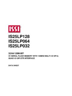
1 IS25LP512M IS25WP512M 512Mb SERIAL FLASH MEMORY 133 MHZ MULTI I/O SPI & QUAD I/O QPI DTR INTERFACE ADVANCED data SHEET IS25LP512M IS25WP512M Integrated Silicon Solution, 2 04/05/2018 FEATURES Industry Standard Serial Interface - IS25LP512M: 512 Mbit/64 Mbyte - IS25WP512M: 512 Mbit/64 Mbyte - 3 or 4 Byte Addressing Mode - Supports Standard SPI, Fast, Dual, Dual I/O, Quad, Quad I/O, SPI DTR, Dual I/O DTR, Quad I/O DTR, and QPI - Software & Hardware Reset - Supports Serial Flash Discoverable Parameters (SFDP) High Performance Serial Flash (SPI) - 80 MHz Normal Read - Up to133 Mhz Fast Read - Up to 80 MHz DTR (Dual Transfer Rate) - Equivalent Throughput of 532 Mb/s - Selectable Dummy Cycles - Configurable Drive Strength - Supports SPI Modes 0 and 3 - More than 100,000 Erase/Program Cycles - More than 20-year data Retention Flexible & Efficient Memory Architecture - Chip Erase with Uniform Sector/Block Erase (4/32/64KB or 4/32/256 KB)(2) - Program 1 to 256 or 512 Byte per Page(2)
2 - Program/Erase Suspend & Resume Efficient Read and Program modes - Low Instruction Overhead Operations - Continuous Read 8/16/32/64 Byte Burst Wrap - Selectable Burst Length - QPI for Reduced Instruction Overhead - AutoBoot Operation - data Learning Pattern for training in DTR operation Low Power with Wide Temp. Ranges - Single Voltage Supply IS25LP: to IS25WP: to - 7 mA Active Read Current - 10 A Standby Current - 1 A Deep Power Down - Temp Grades: Extended: -40 C to +105 C Auto Grade (A3): -40 C to +125 C ADVANCED Security Protection - Software and Hardware Write Protection - ADVANCED Sector/Block Protection - Top/Bottom Block Protection - Power Supply Lock Protection - 4x256 Byte Dedicated Security Area with OTP User-lockable Bits - 128 bit Unique ID for Each Device (Call Factory) Industry Standard Pin-out & Packages(1) - M =16-pin SOIC 300mil(2) - L = 8-contact WSON 8x6mm(2) - G = 24-ball TFBGA 6x8mm (4x6 ball array)(2) - H = 24-ball TFBGA 6x8mm (5x5 ball array)(2) Notes: 1.
3 Call Factory for other package options available. 2. For optional 512 Byte Page size with 256 KB Block size, see the Ordering Information. 512Mb SERIAL FLASH MEMORY 133 MHZ MULTI I/O SPI & QUAD I/O QPI DTR INTERFACE ADVANCED INFORMATION IS25LP512M IS25WP512M Integrated Silicon Solution, 3 04/05/2018 GENERAL DESCRIPTION The IS25LP512M and IS25WP512M Serial Flash memory offers a versatile storage solution with high flexibility and performance in a simplified pin count package. ISSI s Industry Standard Serial Interface Flash is for systems that require limited space, a low pin count, and low power consumption. The device is accessed through a 4-wire SPI Interface consisting of a Serial data Input (SI), Serial data Output (SO), Serial Clock (SCK), and Chip Enable (CE#) pins, which can also be configured to serve as multi-I/O (see pin descriptions).
4 The device supports Dual and Quad I/O as well as standard, Dual Output, and Quad Output SPI. Clock frequencies of up to 133 MHz allow for equivalent clock rates of up to 532 MHz (133 MHz x 4) which equates to of data throughput. The IS25xE series of Flash adds support for DTR (Double Transfer Rate) commands that transfer addresses and read data on both edges of the clock. These transfer rates can outperform 16-bit Parallel Flash memories allowing for efficient memory access to support XIP (execute in place) operation. The memory array is organized into programmable pages of 256/512 bytes. This family supports page program mode where 1 to 256/512 bytes of data are programmed in a single command. QPI (Quad Peripheral Interface) supports 2-cycle instruction further reducing instruction times. Pages can be erased in groups of 4 Kbyte sectors, 32 Kbyte blocks, 64K/256 Kbyte blocks, and/or the entire chip. The uniform sector and block architecture allows for a high degree of flexibility so that the device can be utilized for a broad variety of applications requiring solid data retention.
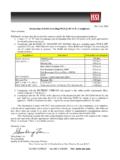
5 Item which must be waived from the initial Engineering Sample Initial Engineering sample does not meet below item in the specification, but it will be fixed in the production version. 1. DTR Function : DTR Read Function does not work for initial Engineering Sample. It will be fixed in the production version. IS25LP512M IS25WP512M Integrated Silicon Solution, 4 04/05/2018 TABLE OF CONTENTS FEATURES .. 2 GENERAL DESCRIPTION .. 3 TABLE OF CONTENTS .. 4 1. PIN CONFIGURATION .. 8 2. PIN DESCRIPTIONS .. 9 3. BLOCK DIAGRAM .. 11 4. SPI MODES DESCRIPTION .. 12 5. SYSTEM CONFIGURATION .. 14 BLOCK/SECTOR ADDRESSES .. 14 Serial Flash Discoverable Parameters .. 16 6. REGISTERS .. 22 STATUS REGISTER .. 22 FUNCTION REGISTER .. 27 READ REGISTER AND EXTENDED REGISTER.
6 28 READ REGISTER .. 28 EXTENDED READ REGISTER .. 30 AUTOBOOT REGISTER .. 32 BANK ADDRESS REGISTER .. 33 ADVANCED SECTOR/BLOCK PROTECTION (ASP) RELATED REGISTER .. 34 ADVANCED SECTOR/BLOCK PROTECTION REGISTER (ASPR) .. 34 PASSWORD REGISTER .. 35 PPB LOCK REGISTER .. 35 PPB REGISTER .. 36 DYB REGISTER .. 36 data LEARNING PATTERN REGISTER .. 37 7. PROTECTION 38 HARDWARE WRITE 38 SOFTWARE WRITE PROTECTION .. 38 BLOCK PROTECTION BITS .. 38 ADVANCED SECTOR/BLOCK PROTECTION (ASP) .. 39 8. DEVICE OPERATION .. 47 COMMAND OVERVIEW .. 47 COMMAND SET SUMMARY .. 48 NORMAL READ OPERATION (NORD, 03h or 4 NORD, 13h) .. 57 FAST READ OPERATION (FRD, 0Bh or 4 FRD, 0Ch) .. 60 HOLD OPERATION .. 64 FAST READ DUAL I/O OPERATION (FRDIO, BBh or 4 FRDIO, BCh) .. 65 FAST READ DUAL OUTPUT OPERATION (FRDO, 3Bh or 4 FRDO, 3Ch).. 69 IS25LP512M IS25WP512M Integrated Silicon Solution, 5 04/05/2018 FAST READ QUAD OUTPUT OPERATION (FRQO, 6Bh or 4 FRQO 6Ch).
7 72 FAST READ QUAD I/O OPERATION (FRQIO, EBh or 4 FRQIO, ECh) .. 75 PAGE PROGRAM OPERATION (PP, 02h or 4PP, 12h).. 82 QUAD INPUT PAGE PROGRAM OPERATION (PPQ, 32h/38h or 4 PPQ, 34h/3Eh) .. 85 ERASE OPERATION .. 86 SECTOR ERASE OPERATION (SER, D7h/20h or 4 SER, 21h) .. 87 BLOCK ERASE OPERATION (BER32K:52h or 4 BER32K:5Ch, BER64K/256K:D8h or 4 BER64K/256K:DCh) .. 89 CHIP ERASE OPERATION (CER, C7h/60h) .. 92 WRITE ENABLE OPERATION (WREN, 06h) .. 93 WRITE DISABLE OPERATION (WRDI, 04h) .. 94 READ STATUS REGISTER OPERATION (RDSR, 05h) .. 95 WRITE STATUS REGISTER OPERATION (WRSR, 01h) .. 96 READ FUNCTION REGISTER OPERATION (RDFR, 48h) .. 97 WRITE FUNCTION REGISTER OPERATION (WRFR, 42h).. 98 ENTER QUAD PERIPHERAL INTERFACE (QPI) MODE OPERATION (QIOEN,35h; QIODI,F5h) .. 99 PROGRAM/ERASE SUSPEND & RESUME .. 100 ENTER DEEP POWER DOWN (DP, B9h) .. 103 RELEASE DEEP POWER DOWN (RDPD, ABh) .. 104 SET READ PARAMETERS OPERATION (SRPNV: 65h, SRPV: C0h/63h).
8 105 SET EXTENDED READ PARAMETERS OPERATION (SERPNV: 85h, SERPV: 83h) .. 107 READ READ PARAMETERS OPERATION (RDRP, 61h) .. 108 READ EXTENDED READ PARAMETERS OPERATION (RDERP, 81h) .. 109 CLEAR EXTENDED READ REGISTER OPERATION (CLERP, 82h) .. 110 READ PRODUCT IDENTIFICATION (RDID, ABh) .. 111 READ PRODUCT IDENTIFICATION BY JEDEC ID OPERATION (RDJDID, 9Fh; RDJDIDQ, AFh) .. 113 READ DEVICE MANUFACTURER AND DEVICE ID OPERATION (RDMDID, 90h) .. 114 READ UNIQUE ID NUMBER (RDUID, 4Bh) .. 115 READ SFDP OPERATION (RDSFDP, 5Ah) .. 116 NO OPERATION (NOP, 00h) .. 116 SOFTWARE RESET (RESET-ENABLE (RSTEN, 66h) AND RESET (RST, 99h)) AND HARDWARE RESET .. 117 SECURITY INFORMATION ROW .. 118 INFORMATION ROW ERASE OPERATION (IRER, 64h) .. 119 INFORMATION ROW PROGRAM OPERATION (IRP, 62h) .. 120 INFORMATION ROW READ OPERATION (IRRD, 68h) .. 121 FAST READ DTR MODE OPERATION (FRDTR, 0Dh or 4 FRDTR, 0Eh) .. 122 FAST READ DUAL IO DTR MODE OPERATION (FRDDTR, BDh or 4 FRDDTR, BEh).
9 127 FAST READ QUAD IO DTR MODE OPERATION IN SPI MODE (FRQDTR, EDh or 4 FRQDTR, EEh) .. 131 IS25LP512M IS25WP512M Integrated Silicon Solution, 6 04/05/2018 SECTOR LOCK/UNLOCK FUNCTIONS .. 139 AUTOBOOT .. 142 READ BANK ADDRESS REGISTER OPERATION (RDBR: 16h/C8h) .. 146 WRITE BANK ADDRESS REGISTER OPERATION (WRBRNV: 18h, WRBRV: 17h/C5h) .. 147 ENTER 4-BYTE ADDRESS MODE OPERATION (EN4B, B7h) .. 148 EXIT 4-BYTE ADDRESS MODE OPERATION (EX4B, 29h) .. 149 READ DYB OPERATION (RDDYB, FAh or 4 RDDYB, E0h) .. 150 WRITE DYB OPERATION (WRDYB, FBh or 4 WRDYB, E1h) .. 152 READ PPB OPERATION (RDPPB, FCh or 4 RDPPB, E2h) .. 154 PROGRAM PPB OPERATION (PGPPB, FDh or 4 PGPPB, E3h) .. 155 ERASE PPB OPERATION (ERPPB, E4h) .. 157 READ ASP OPERATION (RDASP, 2Bh).
10 158 PROGRAM ASP OPERATION (PGASP, 2Fh) .. 159 READ PPB LOCK BIT OPERATION (RDPLB, A7h) .. 160 WRITE PPB LOCK BIT OPERATION (WRPLB, A6h) .. 161 SET FREEZE BIT OPERATION (SFRZ, 91h) .. 162 READ PASSWORD OPERATION (RDPWD, E7h) .. 163 PROGRAM PASSWORD OPERATION (PGPWD, E8h) .. 164 UNLOCK PASSWORD OPERATION (UNPWD, E9h) .. 165 GANG SECTOR/BLOCK LOCK OPERATION (GBLK, 7Eh) .. 166 GANG SECTOR/BLOCK UNLOCK OPERATION (GBUN, 98h) .. 167 data LEARNING PATTERN (DLP).. 168 PROGRAM NVDLR OPERATION (PNVDLR, 43h) .. 171 WRITE VDLR OPERATION (WRVDLR, 4Ah) .. 172 READ DLP OPERATION (RDDLP, 41h) .. 173 9. ELECTRICAL CHARACTERISTICS .. 174 ABSOLUTE MAXIMUM RATINGS (1) .. 174 OPERATING RANGE .. 174 DC CHARACTERISTICS .. 175 AC MEASUREMENT CONDITIONS .. 176 Pin CAPACITANCE .. 176 AC CHARACTERISTICS .. 177 SERIAL INPUT/OUTPUT TIMING .. 179 POWER-UP AND POWER-DOWN .. 181 PROGRAM/ERASE PERFORMANCE .. 182 RELIABILITY CHARACTERISTICS .. 182 10.