Transcription of 液晶ディスプレイ用Al-Nd系合金配線薄膜および 同合金ス …
1 FEATURE : Electronic Materials Al-Nd .. Developments in Al-Nd Alloy Interconnections and Sputtering Targets for Liquid Crystal Displays Dr. Takashi Onishi Eiji Iwamura Katsutoshi Takagi Kazuo Yoshikawa Al-Nd alloy films were developed for the interconnection of advanced liquid crystal displays. Microstructure and its change upon heating of Al-Nd alloy films directly affect stress relaxation behavior. Solid-solution hard- ening and controlling Al film stress relaxation by maintaining Nd at 2 in the alloy were found to be effective in suppressing hillocks up to 400 . Al-Nd alloy films exhibit low electrical resistivity less than 6 cm after the heating and form a high-quality insulation layer under anodization. The results indicate that Al-Nd alloy films are suitable for LCD interconnections and their practical application is promising . LCD . 14 . 15 .. 1 . 3 . Al LSI . LCD Ti Cr Mo Ta Al . 4 . 7 .. 50 cm LCD.
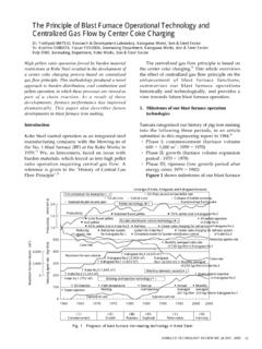
2 Al Al 10 m 200 . Al . LCD 300 400 . LCD .. TFT . LCD . 8 . 9 . Al-Ta Thin Film Transistor : TFT TFT-LCD. 400 6 cm . 10 cm LCD . LCD LCD 1 . LCD . 10 . 11 2 . TFT . 6 . cm Al-Nd . Al-Nd .. 1 Al .. LCD .. 1. SEM . m . 1 400 1h Al . 12 . 13 . SEM . Photo 1 SEM micrograph of hillock formed on pure Al Pb Al films after annealing at 400 for 1h /Vol. 48 No. 3 Dec. 1998 29. Semiconductor (a-Si) 200. Cooling Source Drain Passivation (SiN) 100. Stress MPa Pixel (ITO). 0. 100 Heating Gate Bus-line (Al) Hillock Generation Gate (Al). 200 Line B Line A (Elastic Glass Substrate Gate Insulator (Anodic Oxide). (Proof Stress) Deformation Stress). 1 300. 0 100 200 300 400 500. Fig. 1 Cross-sectional view of a TFT-LCD. Temperature . 2 Al . Fig. 2 Stress-temperature curve of pure Al films LCD . 30. LineWidth 10 m 2. Hillock Density 10 . Line Length 10 mm . 9. Film Thickness 300 nm Annealing Time 1 h 20. 2 Al-Nd . 10.. 12 16 19 0.
3 0 100 200 300 400 500. Annealing Temperature . 3 Al .. 2 Al Fig. 3 Relation between annealing temperature and hillock density for pure Al films . 5. A B Line Length 10mm 2. Hillock Density 10 . Film Thickness 300nm proof stress 4. 9. Annealing 400 1h SEM Scanning Electron 3. Microscopy Ta 2.. Al 150 1 Nd . 0. 150 0 1 2 3 4. SEM Nd, Ta Content at . Al . 20 4 Al Nd Ta . Fig. 4 Relation between Nd Ta content and hillock density for Al alloy films . B . 21 . Al . Nd . Ta Al . Al 4 Nd Ta . 150 2 at . Al . Al-2 . 0 at Nd Al-2 . 0 at Ta Al . 3 Al 5 Al-2 . 0. 1h at Ta Al . 300 . 400 320 . Al Ta . 150 Al3Ta . XRD X-ray Diffractometry . Al-2 . 0 at Ta . 30 KOBE STEEL ENGINEERING REPORTS/Vol. 48 No. 3 Dec. 1998 . 300 (a) at Nd (b) at Ta at Nd Cooling at Ta (As-deposited) (As-deposited). 200. Stress MPa 100. 0. 100. (c) at Nd (d) at Ta 200 Heating (Annealed at 300 ) (Annealed at 300 ). Nd Precipitation 300. Hillock Formation Ta Precipitation 400 Line B (Proof Stress) Line A (Elastic Deformation Stress).
4 0 100 200 300 400 500 100nm Temperature . 5 Al 2 Al TEM . Fig. 5 Stress-temperature curves of Al alloy films Photo 2 TEM micrographs of as-deposited and annealed Al alloy films . 9 . Ta Nd Al-2 . 0 at Nd Al-2 . 0 at Al . Ta . Al-2 . 0 at Nd . 100 Al-Nd Al-Ta .. Al-2 . 0 at Nd Al-2 . 0 at Ta . 100 as-deposited 300 TEM. 2 . Transmission Electron Microscopy . Nd Al4Nd as-deposited . 25nm 30nm . Al-Nd -Al Nd . Al Nd Ta Ta -Al . Nd Ta . Ta . XAFS X-ray Absorption Fine Structure . Ta 6 6 . Al Al-Ta Al-Nd XAFS . 22 . Ta Nd . 3 4at Ta Ta Nd . Ta . 23 . Nd Ta Nd . 24 . 100 Al . 7 -Al Al3Ta Al4Nd . Ta Nd . Ta Nd 25 . 26 . Nd 2 at . Ta Nd . Al-Ta . Al-Nd Al-Ta -Al . Al-Ta system Al-Nd system 18 18. Interatomic Distance . Interatomic Distance . Coordination Number Al3Nd Al3Nd 16 16. Coordination Number Coordination Number Interatomic Distance 14 14 -Al -Al 12 12. 3 3. 10 -Al 10 -Al 6 XAFS Al-Ta Al- 8 Al3Ta 8 Nd Coordination Number 6 6 Interatomic Distance Fig.
5 6 Structural parameters of Al-Ta Al3Ta and Al-Nd alloy films obtained 4 4. 0 5 10 15 20 25 0 5 10 15 20 25. through analysis of XAFS signals Ta Content at Nd Content at . /Vol. 48 No. 3 Dec. 1998 31. Al3Ta Al4Nd Al Ta Nd .. 3 Al-Nd .. Al 8 Al-Nd Al-Ta .. 100 m 10mm 4 .. as-deposited . Al-Nd . 1st Al-Al 12 1st Ta-Al 4 1st Nd-Al 8. 2nd Ta-Al 8 2nd Nd-Al 8 Al-Ta . 7 -Al Al3Ta Al4Nd . 3 . 70 cm/at 8 . 64 . Fig. 7 Crystal structures of -Al Al3Ta and Al4Nd cm/at . -Al Ta Al . Al3Ta -Al . 20 at Nd Ta . 20 at Ta DV-X . -Al Al d . Al3Ta Al . Ta-Al Al . 27 . Al-Ta Al .. Al-Nd Ta . -Al Nd . Nd Al . 28 .. Al4Nd Al-Nd Al-Nd Al-Ta . 10 at Al4Nd Al-Ta 9. Al-Nd Al-2 . 0 at . Al-Nd Al-Ta Ta 1h . Al-2 . 0 at Ta . Al4Nd Al3Ta . 26 . 50. Al-Nd Al-Ta Resistivity cm 40. as-deposited . 300 30. Al-2 . 0 at Nd -Al . 20. 3 Al4Nd . 2 c 10.. 200 300 . 0. Nd 0 1 0 3 4 5 6. 24 Metal Element Content at .. 8 Al . -Al . Fig. 8 Resistivity of as-deposited Al alloy films as a function of Al-2.
6 0 at Nd metal element content Al-2 . 0 at Ta . 25. at Nd Resistivity cm at Nd Al3Ta -Al 20. at Nd at Ta Ta 15.. 10.. 5.. Al-Nd Al-Ta 0. 0 100 200 300 400 500. Annealing Temperature . 9 Al . Fig. 9 Annealing temperature dependence of resistivity for Al alloy films 32 KOBE STEEL ENGINEERING REPORTS/Vol. 48 No. 3 Dec. 1998 . 200 Electric Breakdown Field Al-Nd 200 300 . 300 . MV/cm 5 cm as-deposited 300 .. Mean Value Nd Pure Al at Ta at Nd . Al . Fig. 10 Electric breakdown field of several kinds of Al alloy films. The limiting anodization voltage was 80V. Al-Nd Al-Ta . 10. 7. 8 (a) Pure Al 10. Drain Current A. 4 Al-Nd (b) at Ta 9. 10 (c) at Nd TFT 10. 10.. 11. 10. 10 10. 12. Al Al-2 . 0 at Nd Al-2 . 0 at Ta 5 0 5 10 15 20 25. Gate Voltage V. Al I-V . 3 Fig. 11 I-V characteristics for MIM capasitor with anodic 2 oxide on different Al alloy films 1 : 9 0 . 2mA/cm 80. V 80V 10. 9. Anodic Film Matrix Metal 10.
7 Secondary Ion Intensity counts/s 8. 10. Al Al . 7. 80V 10. 6. 10. Nd 2 at Al . Nd Al Ta 2 at 10. 5. Al . O. I-V 11 10. 4. I-V Al . 3. Al 10. 0 500 1 000 1 500 2 000. Al Ta 2 . 0 at Al Sputtering Time s Nd 2 . 0 at at Nd .. Al Al . Fig. 12 SIMS depth profile of an anodic film formed on an Al-2 0 at Nd alloy film at 80 V anodization voltage Al-2 . 0 at Nd . 9. 10. Secondary Ion Intensity counts/s Anodic Film Matrix Metal . 8. Al 10. Al X . 7. 10.. 6. 10. 5. 10 Ta 4 O. 10.. SIMS Secon- 3. 10. dary Ion Mass Spectrometry 0 500 1 000 1 500 2 000. Sputtering Time s 12 13 SIMS .. O2 -8 KeV-30nA Al Al-2 0at Ta .. Fig. 13 SIMS depth profile of an anodic film formed on an Nd Ta Nd Al-2 0 at Ta alloy film at 80 V anodization voltage /Vol. 48 No. 3 Dec. 1998 33. Al-Nd . Al-Nd . Ta . Al Ta Al . Al-2 . 0 at Ta Al Ta O . Al Al-Nd Al2O3 . XPS X-ray Photoelectron Spec- LCD . troscopy Nd Ta TFT-LCD . Ta LCD . Nd 0 . 5 1.
8 5at .. XRD Al-2 . 0at Nd . 1 M. Yamamoto et al. Conference Record of 1994 Interna- Al2O3 Nd2O3 tional Display Research Conference and International Work- Al-2 . 0 at Ta shop on Active-matrix LCDs & Display Materials 1994 . Al2O3 TaO 2 T. Tsukada : Proceedings of the 12th International Display Research Conference Japan Display '92 1992 . 3 V. Hall et al. Digest of Technical Papers Display Manufac- Al-2 . 0 at Nd turing Technology Conference 1995 . 4 D. E. Castleberry et al. 1988 Society for Information Display International Symposium Digest of Technical Papers SID'88.. Digest 1988 . Al 5 H. Tanaka et al. 1987 Society for Information Display Inter- national Symposium Digest of Technical Papers SID'87 Di- gest 1987 . Al-2 . 0 at Nd . 6 K. Suzuki et al. 1983 Society for Information Display Inter- naional Symposium Digest of Technical Papers SID'83 Di- gest 1983 . 7 M. Ikeda et al. J Appl. Phys. 1989 . 5 Al-Nd 8 E.
9 Iwamura et al. Thin Solid Films 1995 . 9 T. Onishi et al. J. Vac. Sci. Technol. A 1996 . Al-Nd TFT-LCD . 10 Semiconductor World 1992 . 11 1996 . 12 P. Chaudhari : J. Appl. Phys. 1974 . LCD 13 P. Chaudhari : IBM J. RES. DEVELOP. March 1969 . 1969 . 14 K. Sato et al. Metal. Trans. Vol. 2 March 1971 . 15 S. K. Lahiri : J. Appl. Phys. 1970 . Al 16 J. E. Sanchez et al. Scripta METALLURGICA 1992 .. 17 R. Venkatraman et al. J. Vac. Sci. Technol. A 1991 . Al 18 D. Gerth et al. Thin Solid Films 1992 . 19 S. Aceto et al. Thin Solid Films 1992 .. 20 E. Iwamura et al. J. Vac. Sci. Technol. A 1994 .. 21 M. Hershkovitz et al. Thin Solid Films 1985 .. 29 . 22 1995 . 23 T. Onishi et al. American Institute of Physics Conference Proceedings 1997 . 24 T. Onishi et al. J. Vac. Sci. Technol. A 1997 .. 25 W. B. Pearson : A Hand Book of Lattice Spacings and Struc- 3 1 3 m tures of Metals and Alloys 1969 Pergamon Press . Al-Nd 26 G.
10 Ferguson : Structure Reports Part 2 1993 . Kluwer Academic Publishers . 300ppm 27 1990 . 28 J. Deutz et al. J. Phys. F : Metal Phys. 1981 . 29 1998 .. 34 KOBE STEEL ENGINEERING REPORTS/Vol. 48 No. 3 Dec. 1998.