Transcription of Analog to Digital Conversion - Measurement …
1 Measurement Computing 10 Commerce Way Norton, MA 02766 (508) 946-5100 TYPESA nalog-to- Digital Converters (ADCs) transform an Analog voltage to a binary number (a series of 1 s and 0 s), and then eventually to a Digital number (base 10) for reading on a meter, monitor, or chart. The number of binary digits (bits) that represents the Digital number determines the ADC resolution. However, the Digital number is only an approximation of the true value of the Analog voltage at a particular instant because the voltage can only be represented (digitally) in discrete steps. How closely the Digital number approximates the Analog value also depends on the ADC resolution. A mathematical relationship conveniently shows how the number of bits an ADC handles determines its specific theoretical resolution: An n-bit ADC has a resolution of one part in 2n. For example, a 12-bit ADC has a resolution of one part in 4,096, where 212 = 4,096. Thus, a 12-bit ADC with a maximum input of 10 VDC can resolve the Measurement into 10 VDC/4096 = VDC = mV.
2 Similarly, for the same 0 to 10 VDC range, a 16-bit ADC resolution is 10/216 = 10/65,536 = mV. The resolution is usually specified with respect to the full-range reading of the ADC, not with respect to the measured value at any particular ADCsA successive-approximation converter, Figure , is composed of a Digital -to- Analog converter (DAC), a single comparator, and some control logic and registers. When the Analog voltage to be measured is present at the input to the comparator, the system control logic initially sets all bits to zero. Then the DAC s most significant bit (MSB) is set to 1, which forces the DAC output to 1/2 of full scale (in the case of a 10-V full-scale system, the DAC outputs V). The comparator then compares the Analog output of the DAC to the input signal, and if the DAC output is lower than the input signal, (the signal is greater than 1/2 full scale), the MSB remains set at 1. If the DAC output is higher than the input signal, the MSB resets to zero.
3 Next, the second MSB with a weight of 1/4 of full scale turns on (sets to 1) and forces the output of the DAC to either 3/4 full scale (if the MSB remained at 1) or 1/4 full scale (if the MSB reset to zero). The comparator once more compares the DAC output to the input signal and the second bit either remains on (sets to 1) if the DAC output is lower than the input signal, or resets to zero if the DAC output is higher than the input signal. The third MSB is then compared the same way and the process continues in order of descending bit weight until the LSB is compared. At the end of the process, the output register contains the Digital code representing the Analog input signal. Successive approximation ADCs are relatively slow because the comparisons run serially, and the ADC must pause at each step to set the DAC and wait for its output to settle. However, Conversion rates easily can reach over 1 MHz. Also, 12 and 16-bit successive-approximation ADCs are relatively inexpensive, which accounts for their wide use in many PC-based data acquisition ®isters+ VinputFigure ( )Fig.
4 Interestingly, this ADC uses a Digital -to- Analog converter and a comparator. The logic sets the DAC to zero and starts counting up, setting each following bit until it reaches the value of the mea-sured input voltage. The Conversion is then finished and the final number is stored in the ADCA nalog to Digital Conversion 2 Measurement Computing 10 Commerce Way Norton, MA 02766 (508) 946-5100 ADCsVoltage-to-frequency ADCs convert the Analog input voltage to a pulse train with the frequency proportional to the amplitude of the input. (See Figure ) The pulses are counted over a fixed period to determine the frequency, and the pulse counter output, in turn, represents the Digital voltage. Voltage-to-frequency converters inherently have a high noise rejection characteristic, because the input signal is effectively integrated over the counting interval. Voltage-to-frequency Conversion is commonly used to convert slow and noisy signals. Voltage-to-frequency ADCs are also widely used for remote sensing in noisy environments.
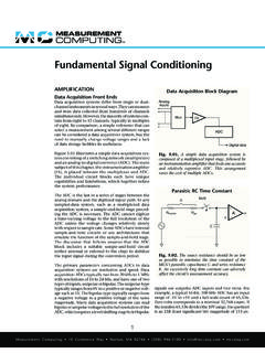
5 The input voltage is converted to a frequency at the remote location and the Digital pulse train is transmitted over a pair of wires to the counter. This eliminates noise that can be introduced in the transmission lines of an Analog signal over a relatively long ADCs: Dual SlopeA number of ADCs use integrating techniques, which measure the time needed to charge or discharge a capacitor in order to determine the input voltage. A widely used technique, called dual-slope integration, is illustrated in Figure It charges a capacitor over a fixed period with a current proportional to the input voltage. Then, the time required to discharge the same capacitor under a constant current determines the value of the input voltage. The technique is relatively accurate and stable because it depends on the ratio of rise time to fall time, not on the absolute value of the capacitor or other components whose values change over temperature and the ADC input over an interval reduces the effect of noise pickup at the ac line frequency when the integration time is matched to a multiple of the ac period.
6 For this reason, it is often used in precision Digital multimeters and panel meters. Although 20-bit accuracy is common, it has a relatively slow Conversion rate, such as 60 Hz maximum, and slower for ADCs that integrate over multiples of the line ADCs A sigma-delta ADC is another type of integrating ADC. It contains an integrator, a DAC, a comparator, and a summing junction. (See Figure ) Like the dual-slope ADC, it s often used in Digital multimeters, panel meters, and data acquisition boards. Sigma-delta converters are relatively inexpensive primarily because they have a single-bit DAC, but they can obtain high-resolution measurements using oversampling techniques. Although the ADC works best with low-bandwidth signals (a few kHz), it typically has better noise rejection than many others, and users can set the integration time (albeit below 100 samples/sec).Sigma-delta ADCs also require few external components. They can accept low-level signals without much input-signal conditioning circuitry for many applications, and they don t require trimming or calibration components because of the DAC s architecture.
7 The ADCs also contain a Digital filter, which lets them work at a high oversampling rate without a separate anti-aliasing filter at the input. Sigma-delta ADCs come in 16 to 24-bit resolution, and they are economical for most data acquisition and instrument ( )IntegrationtimeDischargetimeFixed dischargecurrent=I VinputVcapacitorVrefVinputTdTiTdTiFig. Dual-slope integrating ADCs provide high-resolu-tion measurements with excellent noise rejection. They inte-grate upward from an unknown voltage and then integrate downward with a known source voltage. They are more accu-rate than single slope ADCs because component errors are washed out during the de-integration period. Dual-Slope ADC Integration andDischarge TimesFigure ( )Digitalpulse trainVinVoltage-to-frequencyconverterTim ingcircuitryDigitaloutputsPulsecounterFi g. Voltage-to-frequency converters reject noise well and frequently are used for measuring slow signals or those in noisy environments. Voltage-to-Frequency ADC +Voutto digitalfilterFigure ( )VinVIOVsIntegratorDACVDACVCOVrefVCOVDAC VDACVCO+Vref1 Vref0 Fig.
8 Integrating converters such as the sigma-delta ADC have both high resolution and exceptional noise rejec-tion. They work particularly well for low-bandwidth measure-ments and reject high-frequency noise as well as 50/60 Hz ADC3 Measurement Computing 10 Commerce Way Norton, MA 02766 (508) 946-5100 principle of operation can be understood from the diagram. The input voltage Vin sums algebraically with the output voltage of the DAC, and the integrator adds the summing point output Vs to a value it stored previously. When the integrator output is equal to or greater than zero, the comparator output switches to logic one, and when the integrator output is less than zero, the comparator switches to logic zero. The DAC modulates the feedback loop, which continually adjusts the output of the com-parator to equal the Analog input and maintain the integrator output at zero. The DAC keeps the integrator s output near the reference voltage level. Through a series of iterations, the output signal becomes a one-bit data stream (at a high sample rate) that feeds a Digital filter.
9 The Digital filter averages the series of logic ones and zeros, determines the bandwidth and settling time, and outputs multiple-bit data. The Digital low-pass filter then feeds the decimation filter, which in turn, decreases the sample rate of the multi-bit data stream by a factor of two for each stage within the filter. For example, a seven-stage filter can provide a sample-rate reduction of AccuracyThe Digital filter shown in Figure inherently improves the ADC s accuracy for ac signals in two ways. First, when the input signal varies (sine wave input) and the system samples the signal at several times the Nyquist value (refer to page 17), the integrator becomes a low-pass filter for the input signal, and a high-pass filter for the quantization noise. The Digital filter s averaging function then lowers the noise floor even further, and combined with the decimation filter, the data stream frequency at the output is reduced. For example, the modulator loop frequency could be in the MHz region, but the output data would be in the kHz region.
10 Second, the Digital filter can be notched at 60 Hz to eliminate power line frequency output data rate from the decimation filter is lower than the initial sample rate but still meets the Nyquist requirement by saving certain samples and eliminating others. As long as the output data rate is at least two times the bandwidth of the signal, the decima-tion factor or ratio M can be any integer value. For example, if the input is sampled at fs, the output data rate can be fs/M without losing information. This technique provides more stable readings. (Refer to the table in Figure for ADC comparisons.)ACCURACY AND RESOLUTIONA ccuracy is one of the most critical factors to consider when specifying an ADC for test and Measurement applications. Unfortunately, it s often confused with resolution, and although related, they are distinctly different. Both topics are discussed in this section in some detail, as well as their relationship to calibration, linearity, missing codes, and vs.