Transcription of AP2337 - Diodes Incorporated
1 SINGLE CHANNEL CURRENT-LIMITED LOAD SWITCH AP2337 Document number: DS35060 Rev. 2 - 2 1 of 10 October 2011 Diodes Incorporated NEW PRODUCT Description The AP2337 is single channel current-limited integrated high-side power switches optimized for hot-swap applications. The devices have fast short-circuit response time for improvedoverall system robustness and provide a complete protection solution for application subject to heavy capacitive loads and the prospect of short circuit. It offers reverse current blocking, over-current, over-temperature and short-circuit protection, as well as controlled rise time and under-voltage lockout functionality. The device is available in SOT23 package.
2 Pin Assignments GND( Top View )3IN1 OUT2 SOT23 Features Input voltage range: Fast short-circuit response time accurate current limiting 110m on-resistance Reverse Current Blocking Built-in soft-start with typical turn-on time Over Current Protection Over Voltage Protection Short circuit and thermal protection ESD protection: 3KV HBM, 300V MM Ambient temperature range: -40 C to 85 C Available in Green Molding Compound (No Br, Sb) Lead Free Finish/ RoHS Compliant (Note 1) UL Recognized, File Number E322375 (to be completed) IEC60950-1 CB Scheme Certified (to be completed) Applications LCD TVs & Monitors Set-Top-Boxes, Residential Gateways Laptops, Desktops, Servers Printers, Docking Stations, HUBs Smart phones, e-Readers Notes: 1.
3 EU Directive 2002/95/EC (RoHS). All applicable RoHS exemptions applied. Please visit our website at Typical Application Circuit FINGNDOUTP ower to F SINGLE CHANNEL CURRENT-LIMITED LOAD SWITCH AP2337 Document number: DS35060 Rev. 2 - 2 2 of 10 October 2011 Diodes Incorporated NEW PRODUCT Pin Descriptions Pin Name Pin Number Descriptions GND 1 Ground OUT 2 Switch output pin IN 3 Voltage input pin Function Block Diagram Thermal SenseOUTGNDUVLOC urrent LimitCurrent SenseDischarge ControlDriverIN+-15usDeglitch TimeReverse Voltage ComparatorReverseCurrent Time Absolute Maximum Ratings Symbol Parameter Ratings Units ESD HBM Human Body Model ESD Protection 3 KV ESD MM Machine Model ESD Protection 300 V VIN Input Voltage V VOUT Output Voltage VIN + V Iload Maximum Continuous Load Current Internal Limited A TJmax Maximum Junction Temperature 150 C TST Storage Temperature
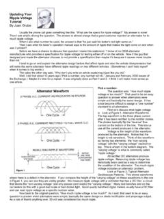
4 Range (Note 2) -65 to 150 C Notes: 2. UL Recognized Rating from -30 C to 70 C ( Diodes qualified TST from -65 C to 150 C) SINGLE CHANNEL CURRENT-LIMITED LOAD SWITCH AP2337 Document number: DS35060 Rev. 2 - 2 3 of 10 October 2011 Diodes Incorporated NEW PRODUCT Recommended Operating Conditions Symbol Parameter Min Max Units VIN Input voltage V IOUT Output Current 0 A TA Operating Ambient Temperature -40 85 C Electrical Characteristics (TA = 25oC, VIN = + , unless otherwise stated) Symbol Parameter Test Conditions (Note 3) Min Unit VUVLO Input UVLO VIN rising IQ Input quiescent current Above UVLO, IOUT= 0 65 110 A IREV Reverse leakage current VIN = 0V, VOUT = 5V, IREV at VIN A RDS(ON) Switch on-resistance VIN = 5V, IOUT = 1A 110 140 m VIN = , IOUT = 1A 140 170 ILIMIT Over-load current limit VIN = 5V, VOUT = 4V, CL=10 F A IOS Short-circuit current OUT connected to ground, CL=10 F A TSHORT Short-circuit response time From VOUT < to IOUT = 0A (OUT shorted to GND) (See Figure.)
5 1)(Note 7) 5 s IROCP Reverse current limit Above UVLO A TTrig Deglitch time from reverse current trigger to MOSFET turn off ms VOVP Output over-voltage trip point Above UVLO (Note 4) 110% 120%VIN TOVP Debounce time from output over-voltage to MOSFET turn off 15 s TON Output turn-on time (Note 5) CL = 1 F, Rload = 5 (UVLO to 90% VOUT-NOM)
6 1 4 ms TDIS Discharge time CL= 1 F, from UVLO to VOUT < 500 s TSHDN Thermal shutdown threshold 150 C THYS Thermal shutdown hysteresis 20 C JA Thermal Resistance Junction-to-Ambient (Note 6) 180 oC/W Notes: 3. Pulse-testing techniques maintain junction temperature close to ambient temperature; thermal effects must be taken into account separately. 4. During output over-voltage protection, the output draws approximately 60 A current. 5. Since the output turn-on slew rate is dependent on input supply slew rate, this limit is only applicable for input supply slew rate between 5 to 5V/1ms. 6. Device mounted on FR-4 substrate PCB, 2oz copper, with minimum recommended pad layout.
7 7. Applicable for output voltage slew rate 5V/30 s. Figure 1. Short Circuit Response Time SINGLE CHANNEL CURRENT-LIMITED LOAD SWITCH AP2337 Document number: DS35060 Rev. 2 - 2 4 of 10 October 2011 Diodes Incorporated NEW PRODUCT Typical Performance Characteristics UVLO Increasing 1ms/div UVLO Decreasing 5ms/div Over-Load Current Limit Short Circuit Current Limit 50ms/div 100us/div Output Over Voltage Trip Point 500us/div Debounce time from output over-voltage to MOSFET turn off (Zoom in at red portion of previous waveform) 20us/div CL=10uFCL=10uFTOVP 12 s OV trip at 114% of Vin, Vin=5V SINGLE CHANNEL CURRENT-LIMITED LOAD SWITCH AP2337 Document number: DS35060 Rev.
8 2 - 2 5 of 10 October 2011 Diodes Incorporated NEW PRODUCT Typical Performance Characteristics (cont.) Deglitch time from reverse current trigger to MOSFET turn off Reverse Current Limit 500us/div 500us/div Output Turn-on Time 1ms/div Discharge Time 5ms/div SINGLE CHANNEL CURRENT-LIMITED LOAD SWITCH AP2337 Document number: DS35060 Rev. 2 - 2 6 of 10 October 2011 Diodes Incorporated NEW PRODUCT Typical Performance Characteristics (cont.) 50556065707580859095-20020406080-40 AMBIENT TEMPERATURE ( C)Fig. 1 Quiescent Supply Current vs. Ambient TemperatureSUPPLY CURRENT ( A) TEMPERATURE ( C)Fig. 2 Short Circuit Output Current vs. Ambient TemperatureSHORT CIRCUIT CURRENT (mA) VOLTAGE (V)Fig.
9 3 Output Turn On-Time vs. Input VoltageC = 1 FR = 5LL 6 OUTPUT TURN ON-TIME (ms) 020406080100120140160180200-20020406080- 40 AMBIENT TEMPERATURE ( C)Fig. 4 Switch On-Resistance vs. Ambient TemperatureON-STATE RESISTANCE (m ) TEMPERATURE ( C)Fig. 5 Current Limit Trip Threshold vs. Ambient TemperatureOVERLOAD CURRENT LIMIT (A)480500520540560580600-20020406080-40 AMBIENT TEMPERATURE ( C)Fig. 6 Reverse Current Limit vs. Ambient TemperatureREVERSE CURRENT LIMIT (mA) SINGLE CHANNEL CURRENT-LIMITED LOAD SWITCH AP2337 Document number: DS35060 Rev. 2 - 2 7 of 10 October 2011 Diodes Incorporated NEW PRODUCT Application Note Protection Features: Under-voltage Lockout (UVLO) Whenever the input voltage falls below UVLO threshold (~ ), the power switch is turned off.
10 This facilitates the design of hot-insertion systems where it is not possible to turn off the power switch before input power is removed. Over-current and Short Circuit Protection An internal sensing FET is employed to check for over-current conditions. Unlike current-sense resistors, sense FETs do not increase the series resistance of the current path. When an overcurrent condition is detected, the device maintains a constant output current and reduces the output voltage accordingly. Complete shutdown occurs only if the fault stays long enough to activate thermal limiting. The different overload conditions and the corresponding response of the AP2337 are outlined below: NO Conditions Explanation Behavior of the AP2337 1 Short circuit condition at start-up Output is shorted before input voltage is applied or before the part is powered up.