Transcription of Chapter 5 Synchronous Sequential Logic
1 15-1 Chapter 5 SynchronousSequential Logic5-2 Outline ! Sequential Circuits!Latches!Flip-Flops!Analysis of Clocked Sequential Circuits!State Reduction and Assignment!Design Procedure25-3 Sequential Circuits !Consist of a combinational circuit to which storage elements are connected to form a feedback path!State the state of the memory devices now, also called current state!Next states and outputs are functions of inputs and present states of storage elements5-4 Two Types of Sequential Circuits ! asynchronous Sequential circuit!Depends upon the input signals at any instantof time and their change order!May have better performance but hard to design! Synchronous Sequential circuit!Defined from theknowledge of its signals atdiscrete instantsof time!Much easier to design(preferred design style)!
2 Synchronized by a periodictrain of clock pulses35-5 Memory Elements!Allow Sequential Logic design!Latch a level-sensitive memory element!SR latches!D latches!Flip-Flop an edge-triggered memory element!Master-slave flip-flop!Edge-triggered flip-flop!RAM and ROM a mass memory element!Discussed in Chapter 75-6 Outline ! Sequential Circuits!Latches!Flip-Flops!Analysis of Clocked Sequential Circuits!State Reduction and Assignment!Design Procedure45-7 Latches!The most basic types of flip-flops operate with signal levels!The basic circuits from which all flip-flops are constructed!Useful for storing binary information and for the design of asynchronous Sequential circuits!Not practical for use in Synchronous Sequential circuits!Avoid to use latches as possible in Synchronous Sequential circuits to avoid design problems5-8SR Latch!
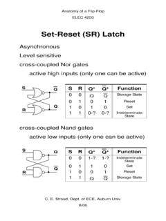
3 A circuit with two cross-coupled NOR gates or two cross-coupled NAND gates!Two useful states:!S=1, R=0 "set state (Q will become to 1)!S=0, R=1 "reset state (Q will become to 0)!When S=0 and R=0 "keep the current value55-9 Undefined State in SR LatchShould be very careful for this case5-10SR Latch with NAND Gates!The SR latches constructed with two cross-coupled NAND gates are active-low!S=1, R=0 "reset state (Q will become to 0)!S=0, R=1 "set state (Q will become to 1)!S=1, R=1 "unchanged65-11SR Latch with Control Input!Add an additional control input to determine when the state of the latch can be changed!C=0: S and R are disabled (no change at outputs)!C=1: S and R are active-high5-12D Latch!D latch has only two inputs: D(data) and C(control)!Use the value of D to set the output value!
4 Eliminate the indeterminate state in the SR latches!The D input goes directly to the S input and its complement is applied to the R input!D=1 "Q=1 "S=1, R=075-13 Graphic Symbols for Latches5-14 Outline ! Sequential Circuits!Latches!Flip-Flops!Analysis of Clocked Sequential Circuits!State Reduction and Assignment!Design Procedure85-15 Flip-Flops!The state of a latch or flip-flop is switched by a change in the control input!This momentary change is called a trigger!Latch: level-sensitive!Flip-Flop: edge-triggered5-16 Latch vs. Flip-Flop!Latch:!Change stored value under specific status of the control signals!Transparent for input signals when control signal is on !May cause combinational feedback loop and extra changes at the output!Flip-Flop:!Can only change stored value by a momentary switch in value of the control signals!
5 Cannot see the change of itsoutput in the same clock pulse!Encounter fewer problemsthan using latches95-17 Master-Slave D Flip-Flop!Constructed with two D latches and an inverter !The first latch (master) is enabled when CLK=1!It reads the input changes but stops before the second one!The second latch (slave) is enabled when CLK=0!Close the first latch to isolate the input changes!Deliver the final value at the moment just before CLK changes!The circuit samples the D input and changes its output Q only at the negative-edgeof the controlling clock5-18 Edge-Triggered D Flip-Flop!If only SR latches are available, three latches are required!Two latches are used for locking the two inputs (CLK & D)!The final latch provides the output of the flip-flop105-19 Setup & Hold Times!
6 The response time of a flip-flop to input changes must be taken into consideration!Setup Time: The length of time that data must stabilize before the clock transition!The maximum data path is used to determine if the setup time is met!Hold Time: The length of time that data must remain stable at the input pin after the active clock transition!The minimum data path is used to determine if hold time is met5-20 Setup & Hold Times!Timing Diagram!Valid Data Transition115-21 Other Flip-Flops!The most economical and efficient flip-flop is the edge-triggered D flip-flop!It requires the smallest number of gates!Other types of flip-flops can be constructed by using the D flip-flop and external Logic !JK flip-flop!T flip-flops!Three major operations that can be performed with a flip-flop:!
7 Set it to 1!Reset it to 0!Complement its output5-22 Edge-Triggered JK Flip-FlopQKJQD''+=K=1:resetJ=1:setJ=0,K= 0: holdJ=1,K=1: toggle125-23 Edge-Triggered T Flip-FlopQTTQQTD''+= =T=0: holdT=1: toggle5-24 Characteristic TablesNo changeResetSetComplementQ(t)01Q (t)01010011Q(t+1)KJJK flip-flopResetSet 0101Q(t+1)DD Flip-FlopNo changeComplement Q(t)Q(t) 01Q(t+1)TT Flip-Flop!Define the logical properties in tabular form135-25 Characteristic Equations !Algebraically describe the next state!Can be derived from characteristic tables!D flip-flop:!JK flip-flop:!T flip-flop:QTTQQTtQ'')1(+= =+QKJQtQ'')1(+=+DtQ=+)1(5-26 Direct Inputs!Force the flip-flop to a particular state immediately!Independent of clock signal!Have higher priority than any other inputs!Useful to bring all flip-flops from unknown into known state while power up!
8 The input that sets the flip-flop to 1 is called presetor direct set!The input that clears the flip-flop to 0 is called clearor direct reset!Also called asynchronous set/reset145-27D F/F with asynchronous Resetother inputs have no effectsdirectly change the internal states of all three latches5-28 Outline ! Sequential Circuits!Latches!Flip-Flops!Analysis of Clocked Sequential Circuits!State Reduction and Assignment!Design Procedure155-29 Sequential Circuit Analysis!The behavior of a clocked Sequential circuit is determined from!The inputs!The outputs!The state of its flip-flops!The outputs and the next state are both a function of the inputs and the present state!To analyze a Sequential circuit, we can use!State equations!State table!State diagram!Flip-Flop input equations5-30 State Equations!
9 Specify the next state as a function of the present state and inputs!Also called transition equation!Analyze the combinationalpart directly!EX:A(t+1) = A(t)x(t) + B(t)x(t)A(t+1) = Ax + BxB(t+1) = A (t) x(t)B(t+1) = A xy(t)=[A(t)+B(t)] x(t)y=(A+B)x A(t+1)A(t)B(t+1)B(t)165-31 State Table!Enumerate the time sequence of inputs, outputs, and flip-flop states!Also called transition table!Similar to list the truth table of state equations!Consist of four sections!Present state, input, next state, and output!A Sequential circuit with m flip-flops and n inputs need 2m+nrows in the state table00111110001100110110000101111010001 0010100000000yBAxBAoutputNext stateinputPresent state5-32 Second Form of State Table!The state table has only three section: present state, next state, and output!
10 The input conditions are enumerated under next state and output sections01010011010100010111001000100000 YYBABABAX=1X=0X=1X=0 StateOutputNext StatePresent175-33 State Diagram!Graphically represent the information in a state table!Circle: a state (with its state value inside)!Directed lines: state transitions (with inputs/outputs above)!Ex: starting from state 00!If the input is 0, it stays at state 00with output=0!If the input is 1, it goes to state 01with output=0!The state table is easier to derivefrom a given Logic diagram andstate equations!The state diagram is suitablefor human interpretation5-34 Flip-Flop Input Equations!To draw the Logic diagram of a Sequential circuit, we need!The type of flip-flops!A list of Boolean expressions of the combinational circuits!