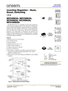
Transcription of Datasheet - XLSEMI芯龙半导体 首页
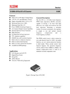
1 Datasheet 150 KHz 100V Buck DC to DC Converter XL7025. Features General Description Maximum Input Voltage 100V The XL7025 is a 150 KHz fixed frequency Output Adjustable from to 20V PWM buck (step-down) DC/DC converter, Maximum Duty Cycle 100% capable of driving a load with high Minimum Drop Out 1V efficiency, low ripple and excellent line and Fixed 150 KHz Switching Frequency load regulation. Requiring a minimum Maximum Output Current number of external components, the Recommend Maximum Output regulator is simple to use and include Current At 5V Output,48V Input internal frequency compensation and a Recommend Maximum Output fixed-frequency oscillator. Current At 15V Output,48V Input Internal Optimize HV Power Transistor The PWM control circuit is able to adjust the High efficiency up to 85% duty ratio linearly from 0 to 100%. An over Excellent line and load regulation current protection function is built inside.
2 Built in thermal shutdown function When output short protection function Built in output short Protection Function happens, the operation frequency will be Built in current limit function reduced from 150 KHz to 45 KHz. An internal TO252-5L package compensation block is built in to minimize external component count. Applications Ebike Controller Power Supply Telecom / Networking Equipment Figure1. Package Type of XL7025. Rev 1. Datasheet 150 KHz 100V Buck DC to DC Converter XL7025. Pin Configurations TO252-5L. 5 OGND. 4 FB. 3 GND. 2 SW. 1 VIN. Metal Tab GND. Figure2. Pin Configuration of XL7025 (Top View). Table 1 Pin Description Pin Number Pin Name Description Supply Voltage Input Pin. Bypass Vin to GND with a suitably 1 VIN. large capacitor to eliminate noise on the input. Power switch Output Pin (SW). Output is the switch node that 2 SW. supplies power to the output. Ground Pin.
3 Care must be taken in layout. This pin should be placed outside of the Schottky Diode to output capacitor 3 GND. ground path to prevent switching current spikes from inducing voltage noise into XL7025. The exposed PAD is GND. Feedback Pin (FB). Through an external resistor divider 4 FB network, Feedback senses the output voltage and regulates it. The feedback threshold voltage is 5 OGND Output Ground Pin. Rev 2. Datasheet 150 KHz 100V Buck DC to DC Converter XL7025. Function Block 120mV 100mV VIN. 8V Regulator 125m . 100mV. Bias current & Start Up Voltage Reference UVLO. COMP2. Current Limit EA. EA. COMP COMP1. FB. RS Latch and Driver switch SW. EA Oscillator 150 KHz/45 KHz OGND. GND. Figure3. Function Block Diagram of XL7025. Typical Application Circuit L1 100uH/1A. VIN SW. 1 2. D1. R2. S210 CFF. XL7025 30K C2 COUT. 33nF. 1% 105 100uF/35V. VIN CIN C1 VOUT. 100uF/100V 104 FB 15V/0~ 4.
4 3 5. GND OGND. R1. R3. 1%.. 1%. OUTPUT 15V/0~ VOUT= *(1+R2/R1). R3 for limit maximum output current, R3 choose in VOUT 5V application; R3 choose in VOUT>5V application. Figure4. XL7025 Typical Application Circuit Rev 3. Datasheet 150 KHz 100V Buck DC to DC Converter XL7025. Ordering Information Order Information Marking ID Package Type Packing Type Supplied As XL7025E1 XL7025E1 TO252-5L 2500 Units on Tape & Reel XLSEMI Pb-free products, as designated with E1 suffix in the par number, are RoHS compliant. Absolute Maximum Ratings Note1 . Parameter Symbol Value Unit Input Voltage Vin to 100 V. Feedback Pin Voltage VFB to Vin V. OGND Pin Voltage VOGND to 7 V. Output switch Pin Voltage VSW to Vin V. Power Dissipation PD Internally limited mW. Thermal Resistance (TO252-5L) o RJA 50 C/W. (Junction to Ambient, No Heatsink, Free Air). o Maximum Junction Temperature TJ -40 to 150 C. o Operating Junction Temperature TJ -40 to 125 C.
5 O Storage Temperature TSTG -65 to 150 C. o Lead Temperature (Soldering, 10 sec) TLEAD 260 C. ESD (HBM) >3000 V. Note1: Stresses greater than those listed under Maximum Ratings may cause permanent damage to the device. This is a stress rating only and functional operation of the device at these or any other conditions above those indicated in the operation is not implied. Exposure to absolute maximum rating conditions for extended periods may affect reliability. Rev 4. Datasheet 150 KHz 100V Buck DC to DC Converter XL7025. XL7025 Electrical Characteristics Ta = 25 ;unless otherwise specified. Symbol Parameter Test Condition Min. Typ. Max. Unit System parameters test circuit figure4. Vin =20V to 80V,Vout=15V. VFB FB Voltage V. Iload= to Vin=36V ,Vout=15V. Efficiency - 86 - %. Iout= Vin=48V ,Vout=15V. Efficiency - 83 - %. Iout= Vin=60V ,Vout=15V. Efficiency - 80 - %. Iout= Electrical Characteristics (DC Parameters).
6 Vin = 48V, GND=0V, Vin & GND parallel connect a 33uf/100V capacitor; Iout= , Ta = 25 ;. the others floating unless otherwise specified. Parameters Symbol Test Condition Min. Typ. Max. Unit Input operation voltage Vin 10 80 V. VIN UVLO Vin_uvlo 8 9 V. Quiescent Supply Current Iq VFB=2V 5 mA. Oscillator Frequency Fosc 120 150 180 KHz VFB=0V. switch Current Limit IL A. R3= . VFB=0V. Output Saturation Voltage VCE V. Iout= Max. Duty Cycle DMAX VFB=0V 100 %. Rev 5. Datasheet 150 KHz 100V Buck DC to DC Converter XL7025. Typical Performance Characteristics Quiescent Supply Current VS Temperature 5. Quiescent Supply Current(mA). 4 VIN=48V. 3. 2. 1. 0. -50 -25 0 25 50 75 100 125. Temperature( ). Figure5. Quiescent Current Curve Feedback Voltage Change VS Temperature VIN=48V,VOUT=5V,IOUT= Feedback Voltage Change(%). Normalized at TA=25 . -50 -25 0 25 50 75 100 125. Temperature( ). Figure6.
7 Feedback Voltage Curve Rev 6. Datasheet 150 KHz 100V Buck DC to DC Converter XL7025. Typical System Application(VOUT=15 ). L1 100uH/1A. VIN SW. 1 2. D1. R2. S210 CFF. XL7025 30K C2 COUT. 33nF. 1% 105 100uF/35V. VIN VOUT. CIN C1. 16V~80V FB 15V/0~ 100uF/100V 104 4. 3 5. GND OGND. R1. R3. 1%.. 1%. INPUT 16V~80V. OUTPUT 15V/0~ VOUT= *(1+R2/R1). Figure7. XL7025 System Application (VIN=16V~80V, VOUT=15 ). Efficiency VS Output current 95. 90. 85. 80. 75. 70. 65. Efficiency(%). 60. 55. VIN=24V,VOUT=15V,IOUT= ~ 50 VIN=36V,VOUT=15V,IOUT= ~ 45 VIN=48V,VOUT=15V,IOUT= ~ 40 VIN=60V,VOUT=15V,IOUT= ~ 35. VIN=72V,VOUT=15V,IOUT= ~ 30. 25. 20. Ouput current(A). Figure8. XL7025 System Application (Efficiency VS Output Current). Rev 7. Datasheet 150 KHz 100V Buck DC to DC Converter XL7025. Typical System Application(VOUT=5 ). L1 100uH/1A. VIN SW. 1 2. D1. R2. S210 CFF. XL7025 10K C2 COUT. 33nF. 1% 105 100uF/16V.
8 VIN VOUT. CIN C1. 10V~80V FB 5V/0~ 100uF/100V 104 4. 3 5. GND OGND. R1. R3. 1%.. 1%. INPUT 10V~80V. OUTPUT 5V/0~ VOUT= *(1+R2/R1). Figure9. XL7025 System Application (VIN=10V~80V, VOUT=5 ). Efficiency VS Output current 90. 85. 80. 75. 70. 65. Efficiency(%). 60. 55. 50 VIN=12V,VOUT=5V,IOUT= ~ VIN=24V,VOUT=5V,IOUT= ~ 45 VIN=36V,VOUT=5V,IOUT= ~ 40 VIN=48V,VOUT=5V,IOUT= ~ VIN=60V,VOUT=5V,IOUT= ~ 35. VIN=72V,VOUT=5V,IOUT= ~ 30. 25. 20. Output current(A). Figure10. XL7025 System Application (Efficiency VS Output Current). Rev 8. Datasheet 150 KHz 100V Buck DC to DC Converter XL7025. Package Information TO252-5L Mechanical Dimensions Rev 9. Datasheet 150 KHz 100V Buck DC to DC Converter XL7025. Important Notice XLSEMI reserve the right to make modifications, enhancements, improvements, corrections or other changes without notice at any time. XLSEMI does not assume any liability arising out of the application or use of any product described herein; neither does it convey any license under its patent rights, nor the rights of others.
9 XLSEMI assumes no liability for applications assistance or the design of Buyers' products. Buyers are responsible for their products and applications using XLSEMI components. To minimize the risks associated with Buyers'. products and applications, Buyers should provide adequate design and operating safeguards. XLSEMI warrants performance of its products to the specifications applicable at the time of sale, in accordance with the warranty in XLSEMI's terms and conditions of sale of semiconductor products. Testing and other quality control techniques are used to the extent XLSEMI deems necessary to support this warranty. Except where mandated by applicable law, testing of all parameters of each component is not necessarily performed. For the latest product information, go to Rev 10.