Example: stock market
Switch Mode Power Supply (SMPS) Topologies
Sep 10, 2007 · Buck Converter A buck converter, as its name implies, can only produce lower average output voltage than the input voltage. The basic schematic with the switching waveforms of a buck converter is shown in Figure 2. In a buck converter, a switch (Q1) is placed in series with the input voltage source V IN. The input source VIN
Tags:
Information
Domain:
Source:
Link to this page:
Documents from same domain

Power Factor Correction in Power Conversion …
ww1.microchip.com© 2007 Microchip Technology Inc. DS01106A-page 2 AN1106 FIGURE 1: CURRENT WAVEFORMS WITH AND WITHOUT PFC These waveforms illustrate that …

2.7V to 5.5V Single Supply CMOS Op Amp
ww1.microchip.comMCP601/1R/2/3/4 DS21314G-page 2 © 2007 Microchip Technology Inc. 1.0 ELECTRICAL CHARACTERISTICS Absolute Maximum Ratings † VDD –VSS.....7.0V

Data Encryption Routines for PIC24 and dsPIC Device
ww1.microchip.com© 2006 Microchip Technology Inc. DS01044A-page 1 AN1044 INTRODUCTION Currently, there are three data encryption standards approved …

Using SAM-BA for Linux on SAMA5D3 Xplained
ww1.microchip.comAN-8995 – Using SAM-BA for Linux on SAMA5D3 Xplained: 42328A−06/2014 Page 5 of 19 2. Setup With Ubuntu distributions, a user has to be member of the dialout group to access serial devices like

MCP6021/1R/2/3/4 - Rail-to-Rail Input/Output, 10 …
ww1.microchip.com2001-2017 Microchip Technology Inc. DS20001685E-page 1 MCP6021/1R/2/3/4 Features • Rail-to-Rail Input/Output • Wide Bandwidth: 10 MHz (typical)

Low Quiescent Current LDO - Microchip Technology
ww1.microchip.com2005-2016 Microchip Technology Inc. DS20001826D-page 1 MCP1700 Features: • 1.6 µA Typical Quiescent Current • Input Operating Voltage Range: 2.3V to 6.0V

MCP1703 250 mA, 16V, Low Quiescent Current
ww1.microchip.com2010 Microchip Technology Inc. DS22049E-page 1 MCP1703 Features: • 2.0 µA Typical Quiescent Current • Input Operating Voltage Range: 2.7V to16.0V

MTCH6102 Low-Power Projected Capacitive Touch …
ww1.microchip.com2014 Microchip Technology Inc. DS40001750A-page 1 Description: Microchip’s MTCH6102 is a turnkey projected capacitive touch controller that simplifies adding

PIC32 GUI Development Board with Projected …
ww1.microchip.comPIC32 GUI Development Board with Projected Capacitance (PCAP) Touch Information Sheet Microchip Technology Inc.

RN4020 Bluetooth Low Energy Module User’s Guide
ww1.microchip.comRN4020 BLUETOOTH LOW ENERGY MODULE USER’S GUIDE 2014 Microchip Technology Inc. DS70005191B-page 7 Preface INTRODUCTION This chapter contains general information that will be useful to know before using the
Related documents

MC34063A - Inverting Regulator - Buck, Boost, Switching 1.5 A
www.onsemi.comInverting Regulator - Buck, Boost, Switching 1.5 A MC34063A, MC33063A, SC34063A, SC33063A, ... 5 4 6 7 Drive 8 Collector Ipk Sense VCC Comparator Inverting Input Switch Switch Emitter Timing Capacitor GND (Bottom View) ... Switch Emitter Voltage (VPin 1 = 40 V) VE(switch) 40 Vdc
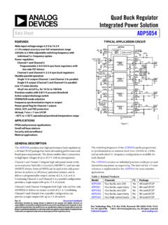
Quad Buck Regulator Integrated Power Solution Data Sheet ...
www.analog.comdischarge switch + – q3 q4 uvlo3 pvin3 sw3 bst3 vreg vreg driver driver pgnd3 control logic and mosfet driver with anticross protection en3 0.8v 1mΩ hiccup and latch-up ocp comp3 0.8v clk3 slope comp clk3 0.72v pwrgd3 zero cross + – + – freq foldback + – + – channel 3—buck duplicate channel 3 channel 4—buck current balance en4 ...

Under the Hood of a DC/DC Boost Converter
www.ti.comUnlike a buck-derived topology, energy flows to the load during the OFF time of the control switch. The effect of any control action during the ON time of the switch is delayed until the switch is turned OFF. For example, during a load-step increase, the output voltage drops due to insufficient stored energy in the inductor. The
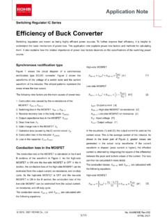
Efficiency of Buck Converter - Rohm
fscdn.rohm.comEfficiency of Buck Converter ... waveforms of the voltage of a switch node and the current waveform of the inductor. The striped patterns represent the areas where the loss occurs. The following nine factors are the main causes of power loss: 1. Conduction loss caused by the on-resistance of the ... 4. Output capacitance loss in the MOSFET ...
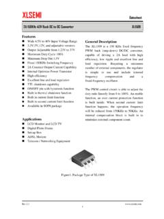
XL1509 Datasheet - xlsemi.com
www.xlsemi.com2A 150KHz 40V Buck DC to DC Converter XL1509 Rev 2.3 www.xlsemi.com ... 3.3V R 2=4 .2K 12V R2=21 .8K Switch 3 Figure3. Function Block Diagram of XL1509 Typical Application Circuit XL1 509-5.0 CIN O C1 1 05 1 80uf 35V D1 L1 68uh/2A +1 2V LOAD 1 5~8 4 2 GND VIN

Switch Mode Power Supply (SMPS) Topologies
ww1.microchip.comSep 10, 2007 · Buck Converter A buck converter, as its name implies, can only produce lower average output voltage than the input voltage. The basic schematic with the switching waveforms of a buck converter is shown in Figure 2. In a buck converter, a switch (Q1) is placed in series with the input voltage source V IN. The input source VIN

Switching regulator fundamentals (Rev. C)
www.ti.comON time of the switch. 2 Switching Converter Topologies The most commonly used DC/DC converter circuits will now be presented along with the basic principles of operation. 2.1 Buck Regulator The most commonly used switching converter is the Buck, which is used to down-convert a DC voltage to a lower DC voltage of the same polarity.

Datasheet - XLSEMI芯龙半导体 首页
xlsemi.com4 5 TO252-5L Metal Tab GND Figure2. Pin Configuration of XL7025 (Top View) Table 1 Pin Description Pin Number Pin Name Description 1 VIN Supply Voltage Input Pin. Bypass Vin to GND with a suitably large capacitor to eliminate noise on the input. 2 SW Power Switch Output Pin (SW). Output is the switch node that supplies power to the output. 3 GND
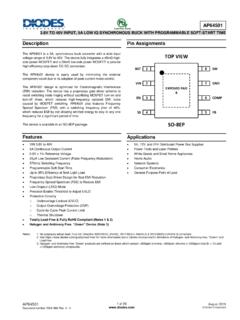
TOP VIEW - Diodes Incorporated
www.diodes.comSW Switch Pin Voltage-0.3 to VIN + 0.3 (DC) V-2.5 to VIN + 2.0 (20ns) T ST Storage Temperature -65 to +150 °C T J Junction Temperature +160 °C T L Lead Temperature +260 °C ESD Susceptibility (Note 5) HBM Human Body Model 2000 V …