Transcription of Low Quiescent Current LDO - Microchip Technology
1 MCP1700. Low Quiescent Current LDO. Features: General Description: A Typical Quiescent Current The MCP1700 is a family of CMOS low dropout (LDO). Input Operating Voltage Range: to voltage regulators that can deliver up to 250 mA of Output Voltage Range: to Current while consuming only A of Quiescent Current (typical). The input operating range is specified 250 mA Output Current for Output from to , making it an ideal choice for two and Voltages three primary cell battery-powered applications, as well 200 mA Output Current for Output as single cell Li-Ion-powered applications. Voltages < The MCP1700 is capable of delivering 250 mA with Low Dropout (LDO) Voltage only 178 mV of input to output voltage differential - 178 mV Typical @ 250 mA for VOUT = (VOUT = ). The output voltage tolerance of the Typical Output Voltage Tolerance MCP1700 is typically at +25 C and 3%.
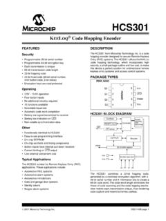
2 Standard Output Voltage Options: maximum over the operating junction temperature - , , , , , , range of -40 C to +125 C. Stable with F Ceramic Output Capacitor Output voltages available for the MCP1700 range from Short Circuit Protection to The LDO output is stable when using only 1 F output capacitance. Ceramic, tantalum or Overtemperature Protection aluminum electrolytic capacitors can all be used for input and output. Overcurrent limit and overtemperature Applications: shutdown provide a robust solution for any application. Battery-Powered Devices Package options include SOT-23, SOT-89, TO-92 and Battery-Powered Alarm Circuits 2x2 DFN-6. Smoke Detectors CO2 Detectors Package Types Pagers and Cellular Phones 3-Pin SOT-23 3-Pin SOT-89. Smart Battery Packs VIN VIN. Low Quiescent Current Voltage Reference 3. PDAs MCP1700. Digital Cameras MCP1700. Microcontroller Power 1 2 3.
3 1 2. GND VOUT GND VIN VOUT. Related Literature: AN765, Using Microchip 's Micropower LDOs 3-Pin TO-92 2x2 DFN-6*. (DS00765), Microchip Technology Inc., 2002 VIN 1 6 VOUT. AN766, Pin-Compatible CMOS Upgrades to MCP1700. BiPolar LDOs (DS00766), NC 2 EP 5 NC. 1 2 3 7. Microchip Technology Inc., 2002 GND 3 4 NC. AN792, A Method to Determine How Much Power a SOT23 Can Dissipate in an Application . (DS00792), Microchip Technology Inc., 2001 GND VIN VOUT. * Includes Exposed Thermal Pad (EP); see Table 3-1. 2005-2016 Microchip Technology Inc. DS20001826D-page 1. MCP1700. Functional Block Diagrams MCP1700. VIN VOUT. Error Amplifier +VIN. Voltage - Reference +. Overcurrent Overtemperature GND. Typical Application Circuits MCP1700. GND VIN. ( to ). VOUT VIN. VOUT CIN. 1 F Ceramic IOUT. 150 mA COUT. 1 F Ceramic DS20001826D-page 2 2005-2016 Microchip Technology Inc. MCP1700.
4 ELECTRICAL Notice: Stresses above those listed under Maximum Ratings may cause permanent damage to the device. This is CHARACTERISTICS a stress rating only, and functional operation of the device at those or any other conditions above those indicated in the Absolute Maximum Ratings operational listings of this specification is not implied. Exposure to maximum rating conditions for extended periods VDD ..+ may affect device reliability. All inputs and outputs .. (VSS - ) to (VIN + ). Peak Output Current .. Internally Limited Storage Temperature ..-65 C to +150 C. Maximum Junction Temperature .. 150 C. Operating Junction C to +125 C. ESD protection on all pins (HBM;MM) 4 kV; 400V. DC CHARACTERISTICS. Electrical Characteristics: Unless otherwise specified, all limits are established for VIN = VR + 1V, ILOAD = 100 A, COUT = 1 F (X7R), CIN = 1 F (X7R), TA = +25 C.
5 Boldface type applies for junction temperatures, TJ (Note 6) of -40 C to +125 C. Parameters Sym. Min. Typ. Max. Units Conditions Input/Output Characteristics Input Operating VIN V Note 1. Voltage Input Quiescent Iq 4 A IL = 0 mA, VIN = VR + 1V. Current Maximum Output IOUT_mA 250 mA For VR Current 200 For VR Output Short IOUT_SC 408 mA VIN = VR + 1V, VOUT = GND. Circuit Current Current (peak Current ) measured 10 ms after short is applied. Output Voltage VOUT VR - VR VR + V Note 2. Regulation VR - VR + VOUT Temperature TCVOUT 50 ppm/ C Note 3. Coefficient Line Regulation VOUT/ + %/V (VR + 1)V VIN 6V. (VOUTX VIN). Load Regulation VOUT/VOUT + % IL = mA to 250 mA for VR IL = mA to 200 mA for VR Note 4. Dropout Voltage VIN - VOUT 178 350 mV IL = 250 mA, (Note 1, Note 5). VR Dropout Voltage VIN - VOUT 150 350 mV IL = 200 mA, (Note 1, Note 5). VR Output Rise Time TR 500 s 10% VR to 90% VR VIN = 0V to 6V, RL = 50 resistive Note 1: The minimum VIN must meet two conditions: VIN and VIN VR + VDROPOUT.
6 2: VR is the nominal regulator output voltage. For example: VR = , , , , , , , , The input voltage VIN = VR + ; IOUT = 100 A. 3: TCVOUT = (VOUT-HIGH - VOUT-LOW) *106 / (VR * Temperature), VOUT-HIGH = highest voltage measured over the temperature range. VOUT-LOW = lowest voltage measured over the temperature range. 4: Load regulation is measured at a constant junction temperature using low duty cycle pulse testing. Changes in output voltage due to heating effects are determined using thermal regulation specification TCVOUT. 5: Dropout voltage is defined as the input to output differential at which the output voltage drops 2% below its measured value with a VR + 1V differential applied. 6: The maximum allowable power dissipation is a function of ambient temperature, the maximum allowable junction temperature and the thermal resistance from junction to air ( , TA, TJ, JA).
7 Exceeding the maximum allowable power dissipation will cause the device operating junction temperature to exceed the maximum 150 C rating. Sustained junction temperatures above 150 C can impact the device reliability. 7: The junction temperature is approximated by soaking the device under test at an ambient temperature equal to the desired Junction temperature. The test time is small enough such that the rise in the Junction temperature over the ambient temperature is not significant. 2005-2016 Microchip Technology Inc. DS20001826D-page 3. MCP1700. DC CHARACTERISTICS (CONTINUED). Electrical Characteristics: Unless otherwise specified, all limits are established for VIN = VR + 1V, ILOAD = 100 A, COUT = 1 F (X7R), CIN = 1 F (X7R), TA = +25 C. Boldface type applies for junction temperatures, TJ (Note 6) of -40 C to +125 C. Parameters Sym. Min. Typ. Max. Units Conditions Output Noise eN 3 V/(Hz)1/2 IL = 100 mA, f = 1 kHz, COUT = 1 F.
8 Power Supply PSRR 44 dB f = 100 Hz, COUT = 1 F, IL = 50 mA, Ripple Rejection VINAC = 100 mV pk-pk, CIN = 0 F, Ratio VR = Thermal TSD 140 C VIN = VR + 1V, IL = 100 A. Shutdown Protection Note 1: The minimum VIN must meet two conditions: VIN and VIN VR + VDROPOUT. 2: VR is the nominal regulator output voltage. For example: VR = , , , , , , , , The input voltage VIN = VR + ; IOUT = 100 A. 3: TCVOUT = (VOUT-HIGH - VOUT-LOW) *106 / (VR * Temperature), VOUT-HIGH = highest voltage measured over the temperature range. VOUT-LOW = lowest voltage measured over the temperature range. 4: Load regulation is measured at a constant junction temperature using low duty cycle pulse testing. Changes in output voltage due to heating effects are determined using thermal regulation specification TCVOUT. 5: Dropout voltage is defined as the input to output differential at which the output voltage drops 2% below its measured value with a VR + 1V differential applied.
9 6: The maximum allowable power dissipation is a function of ambient temperature, the maximum allowable junction temperature and the thermal resistance from junction to air ( , TA, TJ, JA). Exceeding the maximum allowable power dissipation will cause the device operating junction temperature to exceed the maximum 150 C rating. Sustained junction temperatures above 150 C can impact the device reliability. 7: The junction temperature is approximated by soaking the device under test at an ambient temperature equal to the desired Junction temperature. The test time is small enough such that the rise in the Junction temperature over the ambient temperature is not significant. TEMPERATURE SPECIFICATIONS. Electrical Characteristics: Unless otherwise specified, all limits are established for VIN = VR + 1V, ILOAD = 100 A, COUT = 1 F (X7R), CIN = 1 F (X7R), TA = +25 C.
10 Boldface type applies for junction temperatures, TJ (Note 1) of -40 C to +125 C. Parameters Sym. Min. Typ. Max. Units Conditions Temperature Ranges Specified Temperature Range TA -40 +125 C. Operating Temperature Range TJ -40 +125 C. Storage Temperature Range TA -65 +150 C. Thermal Package Resistance Thermal Resistance, 2x2 DFN JA 91 C/W EIA/JEDEC JESD51-7. JC 19 C/W FR-4 4-Layer Board Thermal Resistance, SOT-23 JA 336 C/W EIA/JEDEC JESD51-7. JC 110 C/W FR-4 4-Layer Board Thermal Resistance, SOT-89 JA 180 C/W EIA/JEDEC JESD51-7. JC 52 C/W FR-4 4-Layer Board Thermal Resistance, TO-92 JA 160 C/W. JC C/W. Note 1: The maximum allowable power dissipation is a function of ambient temperature, the maximum allowable junction temperature and the thermal resistance from junction to air ( , TA, TJ, JA). Exceeding the maximum allowable power dissipation will cause the device operating junction temperature to exceed the maximum 150 C rating.