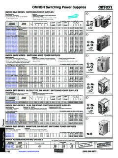
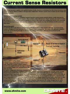
Transcription of Design Guide for QR Flyback Converter
1 Design Note DN 2013-01 January 2013 Design Guide for QR Flyback Converter Allan A. Saliva Infineon Technologies North America (IFNA) Corp. Design Guide for QR Flyback 2 Design Note DN 2013-01 January 2013 Edition 2013-01 Published by Infineon Technologies North America 27703 Emperor Blvd, suite 310, Durham, NC 27703 Infineon Technologies North America Corp. 2013 All Rights Reserved. Attention please! THE INFORMATION GIVEN IN THIS APPLICATION NOTE IS GIVEN AS A HINT FOR THE IMPLEMEN-TATION OF THE INFINEON TECHNOLOGIES COMPONENT ONLY AND SHALL NOT BE REGARDED AS ANY DESCRIPTION OR WARRANTY OF A CERTAIN FUNCTIONALITY, CONDITION OR QUALITY OF THE INFINEON TECHNOLOGIES COMPONENT. THE RECIPIENT OF THIS APPLICATION NOTE MUST VERIFY ANY FUNCTION DESCRIBED HEREIN IN THE REAL APPLICATION.
2 INFINEON TECHNOLOGIES HEREBY DISCLAIMS ANY AND ALL WARRANTIES AND LIABILITIES OF ANY KIND (INCLUDING WITHOUT LIMITATION WARRANTIES OF NON-INFRINGEMENT OF INTELLECTUAL PROPERTY RIGHTS OF ANY THIRD PARTY) WITH RESPECT TO ANY AND ALL INFORMATION GIVEN IN THIS APPLICATION NOTE. Information For further information on technology, delivery terms and conditions and prices please contact your nearest Infineon Technologies Office ( ). Warnings Due to technical requirements components may contain dangerous substances. For information on the types in question please contact your nearest Infineon Technologies Office. Infineon Technologies Components may only be used in life-support devices or systems with the express written approval of Infineon Technologies, if a failure of such components can reasonably be expected to cause the failure of that life-support device or system, or to affect the safety or effectiveness of that device or system.
3 Life support devices or systems are intended to be implanted in the human body, or to support and/or maintain and sustain and/or protect human life. If they fail, it is reasonable to assume that the health of the user or other persons may be endangered. DN 2013-01 Subjects: Fixed Frequency Flyback Author: Allan A. Saliva (IFNA PMM SMD AMR PMD 2) We Listen to Your Comments Any information within this document that you feel is wrong, unclear or missing at all? Your feedback will help us to continuously improve the quality of this document. Please send your proposal (including a reference to this document) to: Design Guide for QR Flyback 3 Design Note DN 2013-01 January 2013 Table of Contents 1. Introduction.
4 4 2. QR Flyback Operation .. 4 3. QR Flyback Design Equations and Sequential Decision Requirements .. 6 4. DCM Flyback Design Example .. 10 5. References: .. 12 Design Guide for QR Flyback 4 Design Note DN 2013-01 January 2013 Figure 2: Free Running QR Flyback Frequency vs Pout 1. Introduction A Quasi-resonant Flyback is simply a DCM Flyback having a valley switching turn on. It is also known as variable frequency or valley switching Flyback and is largely used in low power SMPS application such as charger, adapter and auxiliary supply. The objective of this paper is to develop a practical, step by step and easy to follow approach in designing an off line QR Flyback power supply.
5 This includes quick component selection Guide , Design knowledge and practical tips for a fast and optimized Design . 2. QR Flyback Operation Figure 1A shows the basic Flyback Converter schematic showing the primary parasitic components Lleak and CD. Lleak is the leakage inductance of the transformer while CD is the total capacitance (Coss + intra-winding capacitance + stray capacitance) of the from drain node. Figure 1B shows the normal VDS waveform of a DCM Flyback where two resonant oscillations can be observed. The higher frequency oscillation 1 happened during the initial turned off of the MOSFET due to the leakage inductance resonating with CD. Oscillation 2 happens when the secondary winding energy declines to zero.
6 During this time both windings are open, thus, Lp resonates with the capacitance at the CD node. Because of this resonance, VDS will experience a minimum valley point, whose minimum value will depend on Flyback reflected voltage VR. By making the controller to turn on at this minimum valley, we then have what is called QR or valley switching Flyback . Depending on the QR controller, the MOSFET can be turned on at different valley of the drain-source voltage (first, second even seventh) depending on the loads. If it is always turn on at the first valley point, it is called free running quasi-resonant mode. For the free running QR, the frequency is adjusted depending on the load. Figure 2 shows the frequency vs.
7 Load relationship; the frequency is minimum at maximum load while increasing at lighter loads. Figure 1: (A) Flyback Converter schematic (B) VDS Waveforms of a DCM Flyback Design Guide for QR Flyback 5 Design Note DN 2013-01 January 2013 The switching frequency of the free running QR is given by: Where: Ipripk- Primary peak current, Lpri- Primary inductance, VRp- Primary reflected voltage (Vout x Np/Ns), Vin- Input voltage and CD-Total capacitance on the drain node In this equation it can also be seen that increasing the input voltage will also increase the switching frequency while a the it is inversely proportional to the primary inductance. The basic QR controller uses the auxiliary winding to detect the valley point.
8 Each time the winding voltage ZC (as shown in Figure 2) goes below to a certain threshold during the MOSFET turn off period, the MOSFET is turned on. This is usually called zero current detection ZCD because it waits for the secondary current to go down to zero before turning on the MOSFET. Benefits of QR Flyback : 1. Lower Turn-on Loss: Since it turns on at the valley the turn on losses due to the discharging of CD is significantly reduced. This makes QR Flyback efficiency higher specially high line/lighter loads compare to a FF Flyback 2. Less Conducted EMI: Due to the ripple voltage appearing across the bulk capacitor, the switching frequency is modulated of QR Flyback is modulated at twice the mains frequency.
9 This causes the spectrum to be spread over the wide frequency band than a single frequency values Given the benefits, there are also some drawbacks. Since this is still effectively a DCM Flyback , peak and RMS current remains higher compared to CCM Flyback . This will results in higher conduction losses on the MOSFET and transformer on the primary, while requiring a larger ripple current rated capacitor at the output. Therefore it is not recommended for higher power, wide range designs exceeding 65W-100W, unless cost is a secondary factor and some other possible benefit, such as use of synchronous rectification on the secondary, is critical to system requirements. Finally, because of the variable frequency of operation with varying line and load condition, a few different Design points need to taken into consideration.
10 The following is a sequential Design Guide for QR Flyback highlighting the similarities and the differences between DCM Flyback Design as well as providing Design tips and practical considerations. ZCRZC1 VBUS+Vds-RZC2 CZCF igure 3: QR Flyback valley detection thogh ZC Equation 1 Design Guide for QR Flyback 6 Design Note DN 2013-01 January 2013 Figure 4: Input Design Parameters Figure 5:List of Reccomended QR Controller Table 5: Recommended QR Controller 3. QR Flyback Design Equations and Sequential Decision Requirements STEP 1: Define and determine system requirements: Every SMPS Design starts in determining the required system requirements and specifications. The following parameters need to be defined and determined.