Transcription of Digital Logic Design - 國立臺灣大學
1 Digital Logic DesignBi Basics Combinational Circuits Sequential CircuitsPu-Jen ChengAdapted from the slides prepared by S. Dandamudi for the book, Fundamentals of Computer Organization and Design . Introduction to Digital Logic Basics Hardware consists of a few simple building blocks These are called Logic gates AND, OR, NOT, .. NAND, NOR, XOR, ..Litb iltiti t Logic gates are built using transistors NOT gate can be implemented by a single transistor AND gate requires 3 transistors Transistors are the fundamental devices Pentium consists of 3 million transistors Compaq Alpha consists of 9 million transistors Now we can build chips with more than 100 million transistorsBasic Concepts Simple gates AND OR NOT Functionality can be expressed by a truth table A truth table lists output for each possible input combination Precedence NOT > AND > OR F = A B + A B= (A (B)) + ((A) B)Basic Concepts (cont.)
2 Additional useful gates NAND NOR XOR NAND = AND + NOT NOR = OR + NOT NOR = OR + NOT XOR implements exclusive-OR function NAND and NOR gates require only 2 transistors AND and OR need 3 transistors!Basic Concepts (cont.) Number of functions With Nlogical variables, we can define22 Nfunctions Some of them are usefulAND NAND NOR XOR AND, NAND, NOR, XOR, .. Some are not useful: Output is always 1 Output is always 0 Number of functions definition is useful in proving completeness propertyBasic Concepts (cont.) Complete sets A set of gates is complete If we can implement any logical function using only the type of gates in the set You can uses as many gates as you want Some example complete sets Some example complete sets {AND, OR, NOT} Not a minimal complete set {AND, NOT} {OR, NOT} {NAND} {NOR} Minimal complete set A complete set with no redundant Concepts (cont.) Proving NAND gate is universal NAND gate is called universal gateBasic Concepts (cont.)
3 Proving NOR gate is universal NOR gate is called universal gateLogic ChipsLogic Chips (cont.) Integration levels SSI (small scale integration) Introduced in late 1960s 1-10 gates (previous examples) MSI (medium scale integration) Introduced in late 1960s 10-100 gates LSI (large scale integration) Introduced in early 1970s 100-10,000 gates VLSI (very large scale integration) Introduced in late 1970s More than 10,000 gatesLogic Functions Logical functions can be expressed in several ways: Truth table Logical expressionsGraphical form Graphical form Example: Majority function Output is 1 whenever majority of inputs is 1 We use 3-input majority functionLogic Functions (cont.)3-input majority functionABCF00000010 Logical expression formF = A B + B C + A C010001111000101111011111 Logical Equivalence All three circuits implement F = A B functionLogical Equivalence (cont.) Proving logical equivalence of two circuits Derive the logical expression for the output of each circuit Show that these two expressions are equivalent Two ways: Two ways: You can use the truth table method For every combination of inputs, if both expressions yield the same output, they are equivalent Good for logical expressions with small number of variables You can also use algebraic manipulation Need Boolean identitiesLogical Equivalence (cont.)
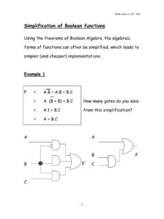
4 Derivation of logical expression from a circuit Trace from the input to output Write down intermediate logical expressions along the pathLogical Equivalence (cont.) Proving logical equivalence: Truth table methodABF1 = A BF3 = (A + B) (A + B) (A + B)000 00100010 0100 0111 1 Boolean AlgebraBoolean Algebra (cont.)Boolean Algebra (cont.) Proving logical equivalence: Boolean algebra method To prove that two logical functions F1 and F2 are equivalent Start with one function and apply Boolean laws to Start with one function and apply Boolean laws to derive the other function Needs intuition as to which laws should be applied and when Practice helps Sometimes it may be convenient to reduce both functions to the same expression Example: F1= A B and F3 are equivalentA B = (A + B) (A + B) (A + B) Logic Circuit Design Process A simple Logic Design process involves Problem specification Truth table derivation Derivation of logical expression Simplification of logical expressionIl tti ImplementationDeriving Logical Expressions Derivation of logical expressions from truth tables sum-of-products (SOP) form product-of-sums (POS) form SOP form WiANDfhibi ih Write an AND term for each input combination that produces a 1 output Write the variable if its value is 1; complement otherwise OR the AND terms to get the final expression POS form Dual of the SOP formDeriving Logical Expressions (cont.)
5 3-input majority functionABCF00000010 SOP logical expression Four product terms Because there are 4 rows with a 1 output010001111000101111011111F = A B C + A B C + A B C + A B CDeriving Logical Expressions (cont.) 3-input majority functionABCF00000010 POS logical expression Four sum terms Because there are 4 rows with a 0 output010001111000101111011111F = (A + B + C) (A + B + C)(A + B + C) (A + B + C)Logical Expression Simplification Two basic methods Algebraic manipulation Use Boolean laws to simplify the expression Difficult to use Don t know if you have the simplified form Karnaugh map (K-map) method Karnaugh map (K-map) method Graphical method Easy to use Can be used to simplify logical expressions with a few variablesAlgebraic Manipulation Majority function exampleA B C + A B C + A B C + A B C =A B C + A B C + A B C + A B C + A B C + A B C Added extra We can now simplify this expression asB C + A C + A B A difficult method to use for complex expressionsKarnaugh Map MethodNote the orderKarnaugh Map Method (cont.)
6 Simplification examplesKarnaugh Map Method (cont.)First and last columns/rows are adjacentKarnaugh Map Method (cont.)Minimal expression depends on groupingsKarnaugh Map Method (cont.)No redundant groupingsKarnaugh Map Method (cont.) Example Seven-segment display Need to select the right LEDs to display a digitKarnaugh Map Method (cont.)Karnaugh Map Method (cont.)Don t cares simplify the expression a lotImplementation Using NAND Gates Using NAND gates Get an equivalent expressionA B + C D = A B + C D Using de Morgan s lawUgd ogaaA B + C D = A B .C D Can be generalized Majority functionA B + B C + AC = A B .BC .ACIdea: NAND Gates: Sum-of-Products, NOR Gates: Product-of-SumsImplementation Using NAND Gates (cont.) Majority functionIntroduction to Combinational Circuits Combinational circuits Output depends only on the current inputs Combinational circuits provide a higher level of abstractionHl i d i d il it Help in reducing Design complexity Reduce chip count We look at some useful combinational circuitsMultiplexers Multiplexer 2ndata inputs n selection inputs a single output4-data input MUX Selection input determines the input that should be connected to the outputMultiplexers (cont.)
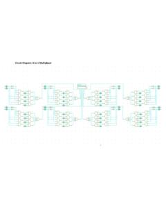
7 4-data input MUX implementationMultiplexers (cont.)MUX implementationsMultiplexers (cont.)Example chip: 8-to-1 MUXM ultiplexers (cont.)Efficient implementation: Majority functionDemultiplexers (DeMUX) Demultiplexer a single input n selection inputs 2noutputsDecoders Decoder selects one-out-of-N inputsDecoders (cont.) Logic function implementationComparator Used to implement comparison operators (= , > , < , , )Comparator (cont.)4-bit magnitude comparator chipA=B: Ox= Ix (x=A<B, A=B, & A>B)Comparator (cont.)Serial construction of an 8-bit comparator1-bit Comparatorxyx>yx=yx<yCMPxyx>y x=yx<y8-bit comparatorxyx>yx=yx<yCMPxn>ynxn=ynxn<ynxyAdders Half-adder Adds two bits Produces a sumand carry Problem: Cannot use it to build larger inputsFlldd Full-adder Adds three 1-bit values Like half-adder, produces a sumand carry Allows building N-bit adders Simple technique Connect Coutof one adder to Cinof the next These are called ripple-carry addersAdders (cont.)
8 Adders (cont.)A 16-bit ripple-carry adderAdders (cont.) Ripple-carry adders can be slow Delay proportional to number of bits Carry lookahead adders Eliminate the delay of ripple-carry adders Carry-ins are generated independently Carryins are generated independently C0= A0B0 C1= A0B0A1+ A0B0B1+ A1B1 .. Requires complex circuits Usually, a combination carry lookahead and ripple-carry techniques are usedProgrammable Logic Arrays PLAs Implement sum-of-product expressions No need to simplify the logical expressions Take Ninputs and produce MoutputsEach input represents a logical variable Each input represents a logical variable Each output represents a logical function output Internally uses An AND array Each AND gate receives 2 Ninputs Ninputs and their complements An OR arrayProgrammable Logic Arrays (cont.)A blank PLA with 2 inputs and 2 outputsProgrammable Logic Arrays (cont.)Implementation examplesProgrammable Logic Arrays (cont.)
9 Simplified notation1-bit Arithmetic and Logic Unit Preliminary ALU design2 s complementRequired 1 is added via Cin1-bit Arithmetic and Logic Unit (cont.)Final designArithmetic and Logic Unit (cont.)16-bit ALUA rithmetic and Logic Unit (cont d)4-bit ALUI ntroduction to Sequential Circuits Output depends on current as well as past inputs Depends on the history Have memory property Sequential circuit consists of Cbii lii Combinational circuit Feedback circuit Past input is encoded into a set of state variables Uses feedback (to feed the state variables) Simple feedback Uses flip flopsIntroduction (cont.)Main components of a sequential circuitClock SignalClock Signal (cont.) Clock serves two distinct purposes Synchronization point Start of a cycle End of a cycleIntermediate point at which the clock signal changes Intermediate point at which the clock signal changes levels Timing information Clock period, ON, and OFF periods Propagation delay Time required for the output to react to changes in the inputsClock Signal (cont.)
10 SR Latches Can remember a bit Level-sensitive (not edge-sensitive)A NOR gate implementation of SR latchSR Latches (cont.) SR latch outputs follow inputs In clocked SR latch, outputs respond at specific instances Uses a clock signalD Latches D Latch Avoids the SR = 11 statePositive Edge-Triggered D Flip-Flops Edge-sensitive devices Changes occur either at positive or negative edgesNotation for Latches & Flip-Flops Not strictly followed in the literatureLatchesFlip-flopsLow level High level Positive edge Negative edgeExample of Shift Register Using D Flip-Flops74164 shiftRegister chipMemory Design Using D Flip-FlopsRequire separate data in and out linesJK Flip-FlopsJK flip-flop (master-slave)J K Qn+100Q0 0 Qn0 1 01 0 11 1 QnExamples of D & JK Flip-FlopsTwo example chipsD latches JK flip-flopsExample of Shift Register Using JK Flip-Flops Shift Registers Can shift data left or right with each clock pulseA 4-bit shift register using JK flip-flopsExample of Counter Using JK Flip-Flops Counters Easy to build using JK flip-flops Use the JK = 11 to toggle Binary counters Simple designpg B bits can count from 0 to 2B 1 Ripple counter Increased delay as in ripple-carry adders Delay proportional to the number of bits Synchronous counters Output changes more or less simultaneously Additional cost/complexityModulo-8 Binary Ripple Counter Using JK Flip-FlopsLSBS ynchronous Modulo-8 Counter Designed using the following simple rule Change output if the preceding count bits are 1 Q1