Transcription of Document Reference No.: FT 000818 Clearance No.: FTDI ...
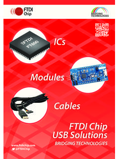
1 Use of FTDI devices in life support and/or safety applications is entirely at the user s risk, and the user agrees to defend, indemnify and hold harmless FTDI from any and all damages, claims, suits or expense resulting from such use. UMFT234XF Datasheet Version Document Reference No.: FT_000818 Clearance No.: FTDI# 337 Future Technology Devices International Ltd Datasheet UMFT234XF Development Module UMFT234XF is a USB to UART development module 1 Introduction The UMFT234XF development module utilizes FTDI s FT234XD IC to convert USB to a basic UART (RXD, TXD, RTS#, CTS#).
2 Features The UMFT234XF is a development module that converts Full-Speed to UART. The module includes a micro-B USB connector to connect to a USB host and the UART IO are available on separate pads. The module is designed to be soldered directly to another PCB (PCB on PCB technology). The UART interface operates between + and + voltage levels depending on the VIO signal, however all I/Os are 5V tolerant. An additional configurable bus (CBUS) pad allows for general IO or indicating that the module is connected to a dedicated charging port for battery charging.
3 Ordering Information Module Interface Features UMFT234XF UART USB full speed to basic UART with one control bus line which may be used for battery charger detection. The PCB pads are designed to be soldered directly to another PCB for secure bonding. 2 Copyright 2013 Future Technology Devices International Limited UMFT234XF Datasheet Version Document Reference No.: FT_000818 Clearance No.: FTDI# 337 2 Driver Support Royalty-Free VIRTUAL COM PORT (VCP): Windows 8 32,64-bit Windows 7 32,64-bit Windows Vista Windows XP 32,64-bit Windows XP Embedded Windows , and MAC OS OS-X Linux and greater Android Royalty-Free D2XX Direct Drivers.
4 Windows 8 32,64-bit Windows 7 32,64-bit Windows Vista Windows XP 32,64-bit Windows XP Embedded Windows , and MAC OS OS-X Linux and greater Android The drivers listed above as well as Third Party Drivers for other operating systems are available for free downloads from 3 Copyright 2013 Future Technology Devices International Limited UMFT234XF Datasheet Version Document Reference No.: FT_000818 Clearance No.: FTDI# 337 Table of Contents 1 Introduction .. 1 Features .. 1 Ordering Information .. 1 2 Driver Support .. 2 3 UMFT234XF Signals and Configurations.
5 4 UMFT234XF CN1 Signal Descriptions .. 4 UMFT234XF PAD Signal Descriptions .. 4 UMFT234XF J-1 .. 4 4 CBUS Signal Options .. 5 Configuring the MTP ROM .. 6 5 Module Dimensions .. 7 6 Module Circuit Schematic .. 8 UMFT234XF Schematic .. 8 7 Environmental Compliances .. 9 8 Internal MTP ROM Configuration .. 10 9 Contact Information .. 11 Appendix A - List of Figures and Tables .. 9 Appendix B: Revision History .. 10 4 Copyright 2013 Future Technology Devices International Limited UMFT234XF Datasheet Version Document Reference No.: FT_000818 Clearance No.
6 : FTDI# 337 3 UMFT234XF Signals and Configurations USB connectivity is via CN1 a micro-B USB connector. The UART and CBUS signals are available on PCB pads. UMFT234XF CN1 Signal Descriptions Pin No. Name Type Description 1 VBUS PWR 5V Power input to USB port, for a USB bus low-powered design; up to 100mA may be sourced from the 5V supply on the USB bus. A maximum of 500mA can be sourced from the USB bus in a USB bus high-powered design. 2 D- Signal Negative USB data signal 3 D+ Signal Positive USB data signal 4 ID Signal Not Connected 5 GND PWR Module Ground Table 1 USB Connector Pin Out Description UMFT234XF PAD Signal Descriptions Pad No.
7 Name Type Description P1 RESET# Signal Active low input may be used to reset the FT234XD IC P2 3V3 PWR 3V3 OUT from FT234XD. May be used for external logic. (50mA max) Also powers the FT234XD VCCIO (if JP1 fitted (default) P3 VIO PWR Optional input to supply the FT234XD VCCIO from an external supply. VIO may be between to JP1 must be disconnected to use this input. P4 GND PWR Module GND P5 VBUS PWR 5V output supplied from the USB port. P6 CB0 Signal Configurable Bus pin 0. Available settings for the pin are defined in table 3. The default is PWREN# P7 TXD Signal UART data output signal P8 RTS# Signal UART Ready to Send output signal.)
8 Active low. P9 RXD Signal UART data input signal P10 CTS# Signal UART Clear to Send input signal. Active low. Table 2 USB Connector Pin Out Description UMFT234XF J-1 J-1 is used to connect/disconnect the 3V3 OUT frm the FT234XD IC to the VCCIO input pin. By default it is connected. 5 Copyright 2013 Future Technology Devices International Limited UMFT234XF Datasheet Version Document Reference No.: FT_000818 Clearance No.: FTDI# 337 4 CBUS Signal Options CBUS Signal Option Available On CBUS Pin Description Tristate CBUS0 IO Pad is tri-stated DRIVE_1 CBUS0 Output a constant 1 DRIVE_0 CBUS0 Output a constant 0 TXDEN CBUS0 Enable transmit data for RS485 PWREN# CBUS0 Output is low after the device is configured by USB but high during USB suspended mode.
9 This output is used to control power to external logic. TXLED# CBUS0 Transmit data LED drive open drain pulses low when transmitting data via UART. RXLED# CBUS0 Receive data LED drive open drain pulses low when receiving data via UART. TX&RXLED# CBUS0 LED drive open drain pulses low when transmitting or receiving data via UART. SLEEP# CBUS0 Goes low during USB suspend mode. Typically used to power down external logic to RS232 level converter IC in USB to RS232 converter designs CLK24 MHz CBUS0 24 MHz Clock output.** CLK12 MHz CBUS0 12 MHz Clock output.
10 ** CLK6 MHz CBUS0 6 MHz Clock output.** GPIO CBUS0 CBUS bit bang mode option. Allows up to 4 of the CBUS pins to be used as general purpose I/O. A separate application note, AN232R-01, available from FTDI website ( ) describes in more detail how to use CBUS bit bang mode. BCD_Charger CBUS0 Battery Charge Detect indicates when the device is connected to a dedicated battery charger host. Active high output. NOTE: Requires a 10K pull-down to remove power up toggling. BCD_Charger# CBUS0 Active low BCD Charger, driven by an open drain to ground with no internal pull-up.