Transcription of E Series Power MOSFET - Vishay Intertechnology
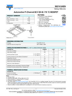
1 Siliconix S15-0399-Rev. E, 16-Mar-151 Document Number: 91482 For technical questions, contact: DOCUMENT IS SUBJECT TO CHANGE WITHOUT NOTICE. THE PRODUCTS DESCRIBED HEREIN AND THIS DOCUMENTARE SUBJECT TO SPECIFIC DISCLAIMERS, SET FORTH AT Series Power MOSFETFEATURES Low figure-of-merit (FOM) Ron x Qg Low input capacitance (Ciss) Reduced switching and conduction losses Ultra low gate charge (Qg) Avalanche energy rated (UIS) Material categorization: for definitions of compliance please see APPLICATIONS Switch mode Power supplies (SMPS) Power factor correction Power supplies (PFC) Lighting- High-intensity discharge (HID)- Fluorescent ballast lighting Industrial- Welding- Induction heating- Motor drives- Battery chargers- Renewable energy- Solar (PV inverters)Notesa.
2 Repetitive rating; pulse width limited by maximum junction VDD = 50 V, starting TJ = 25 C, L = mH, Rg = 25 , IAS = 12 mm from ISD ID, dI/dt = 30 A/ s, starting TJ = 25 SUMMARYVDS (V) at TJ (on) max. at 25 C ( )VGS = 10 V max. (nC)362 Qgs (nC)48 Qgd (nC)98 ConfigurationSingleN-Channel MOSFET GDSTO-247 ACGDSA vailableORDERING INFORMATIONP ackageTO-247 ACLead (Pb)-freeSiHG73N60E-E3 Lead (Pb)-free and Halogen-free SiHG73N60E-GE3 ABSOLUTE MAXIMUM RATINGS (TC = 25 C, unless otherwise noted)PARAMETER SYMBOLLIMITUNITD rain-Source VoltageVDS600V Gate-Source VoltageVGS 30 Continuous Drain Current (TJ = 150 C)
3 VGS at 10 VTC = 25 C ID73 ATC = 100 C 46 Pulsed Drain Current aIDM 236 Linear Derating C Single Pulse Avalanche Energy bEAS 2030mJ Maximum Power DissipationPD520W Operating Junction and Storage Temperature RangeTJ, Tstg-55 to +150 C Drain-Source Voltage SlopeVDS = 0 V to 80 % VDSdV/dt60V/nsReverse Diode dV/dt Recommendations (Peak Temperature) cfor 10 s300 C Siliconix S15-0399-Rev. E, 16-Mar-152 Document Number: 91482 For technical questions, contact: DOCUMENT IS SUBJECT TO CHANGE WITHOUT NOTICE. THE PRODUCTS DESCRIBED HEREIN AND THIS DOCUMENTARE SUBJECT TO SPECIFIC DISCLAIMERS, SET FORTH AT Coss(er) is a fixed capacitance that gives the same energy as Coss while VDS is rising from 0 % to 80 % Coss(tr) is a fixed capacitance that gives the same charging time as Coss while VDS is rising from 0 % to 80 % RESISTANCE RATINGSPARAMETER Junction-to-AmbientRthJA-40 C/WMaximum Junction-to-Case (Drain) (TJ = 25 C, unless otherwise noted)
4 PARAMETER SYMBOLTEST CONDITIONS Breakdown Voltage VDS VGS = 0 V, ID = 250 A 600--V VDS Temperature Coefficient VDS/TJ Reference to 25 C, ID = 250 C Gate-Source Threshold Voltage (N)VGS(th)VDS = VGS, ID = 250 A 2-4V Gate-Source Leakage IGSS VGS = 20 V-- 100nA VGS = 30 V-- 1 A Zero Gate Voltage Drain Current IDSS VDS = 600 V, VGS = 0 V --1 A VDS = 480 V, VGS = 0 V, TJ = 125 C --10 Drain-Source On-State Resistance RDS(on) VGS = 10 VID = 36 Forward Transconductance gfs VDS = 40 V, ID = 10 A-12-S DynamicInput Capacitance Ciss VGS = 0 V, VDS = 100 V, f = 1 MHz-7700-pF Output Capacitance Coss -320-Reverse Transfer Capacitance Crss -5-Effective Output Capacitance, Energy Related aCo(er) VDS = 0 V to 480 V, VGS = 0 V -259-Effective Output Capacitance, Time Related bCo(tr)
5 -907-Total Gate Charge Qg VGS = 10 V ID = 24 A, VDS = 480 V-241362nC Gate-Source Charge Qgs -48-Gate-Drain ChargeQgd -98-Turn-On Delay Time td(on) VDD = 480 V, ID = 24 A, VGS = 10 V, Rg = 10 -6395nsRise Timetr -105158 Turn-Off Delay Time td(off) -290435 Fall Time tf -120180 Gate Input Resistance Rgf = 1 MHz, open Drain-Source Body Diode CharacteristicsContinuous Source-Drain Diode Current ISMOSFET symbolshowing the integral reverse p - n junction diode--73 APulsed Diode Forward CurrentISM--200 Diode Forward VoltageVSDTJ = 25 C, IS = 36 A, VGS = 0 Recovery TimetrrTJ = 25 C, IF = IS = 24 A,dI/dt = 100 A/ s, VR = 25 V-6571314nsReverse Recovery CReverse Recovery Siliconix S15-0399-Rev.
6 E, 16-Mar-153 Document Number: 91482 For technical questions, contact: DOCUMENT IS SUBJECT TO CHANGE WITHOUT NOTICE. THE PRODUCTS DESCRIBED HEREIN AND THIS DOCUMENTARE SUBJECT TO SPECIFIC DISCLAIMERS, SET FORTH AT CHARACTERISTICS (25 C, unless otherwise noted) Fig. 1 - Typical Output Characteristics Fig. 2 - Typical Output Characteristics Fig. 3 - Typical Transfer Characteristics Fig. 4 - Normalized On-Resistance vs. Temperature Fig. 5 - Typical Capacitance vs. Drain-to-Source Voltage Fig. 6 - Coss and Eoss vs. VDSVDS, Drain-to-Source Voltage (V)ID, Drain-to-Source Current (A)0 5 10 15 20 25 30 0 50 100 150 200 250 TJ = 25 CTOP 15 V14 V13 V12 V11 V10 V 5 V6 V7 V8 V9 VVDS, Drain-to-Source Voltage (V)ID, Drain-to-Source Current (A)0102051525300 30 60 90 120 150 5 V6 V7 VTOP 15 V14 V13 V12 V11 V10 V 9 V 8 VTJ = 150 CVGS, Gate-to-Source Voltage (V)
7 ID, Drain-to-Source Current (A)01025515200 50 100 150 200 250 TJ = 25 CTJ = 150 CTJ, Junction Temperature ( C)RDS(on), 40 - 20020 40 60 80 100 120140160 VGS = 10 VID = 36 AOn Resistance (Normalized) VDS, Drain-to-Source Voltage (V)Capacitance (pF)10010020040010 00011000100300500600 CissCossCrss VGS = 0 V, f = 1 MHzCiss = Cgs + Cgd, Cds ShortedCrss = CgdCoss = Cds + Cgd100 000051015202530354045 20 200 20000100200300400500600 Eoss( J)Coss(pF) Siliconix S15-0399-Rev. E, 16-Mar-154 Document Number: 91482 For technical questions, contact: DOCUMENT IS SUBJECT TO CHANGE WITHOUT NOTICE. THE PRODUCTS DESCRIBED HEREIN AND THIS DOCUMENTARE SUBJECT TO SPECIFIC DISCLAIMERS, SET FORTH AT Fig. 7 - Typical Gate Charge vs. Gate-to-Source Voltage Fig.
8 8 - Typical Source-Drain Diode Forward Voltage Fig. 9 - Maximum Safe Operating Area Fig. 10 - Maximum Drain Current vs. Case Temperature Fig. 11 - Temperature vs. Drain-to-Source VoltageQg, Total Gate Charge (nC)VGS, Gate-to-Source Voltage (V)164 024201280 60 120 180 240 300 360 420 480 VDS = 480 VVDS = 300 VVDS = 120 VVSD, Source-Drain Voltage (V)ISD, Reverse Drain Current (A) 1 10 100 1000 1 TJ = 150 CTJ = 25 CVGS = 0 VVDS, Drain-to-Source Voltage (V)ID, Drain Current (A)* VGS > minimum VGS at which RDS(on) is specified 1 10 100 1000 1 10 100 1000 1 ms IDM Limited BVDSS Limited 10 ms 100 s Limited by RDS(on)
9 *TC = 25 CTJ = 150 CSingle PulseOperation in this AreaLimited by RDS(on) TJ, Case Temperature ( C)ID, Drain Current (A)2550751001251501020304050607080 0TJ, Junction Temperature ( C)VDS, Drain-to-Source675600- 600160725 Breakdown Voltage (V)700650625575- 40 - 2020 40 60 80 100 120 Siliconix S15-0399-Rev. E, 16-Mar-155 Document Number: 91482 For technical questions, contact: DOCUMENT IS SUBJECT TO CHANGE WITHOUT NOTICE. THE PRODUCTS DESCRIBED HEREIN AND THIS DOCUMENTARE SUBJECT TO SPECIFIC DISCLAIMERS, SET FORTH AT Fig. 12 - Normalized Thermal Transient Impedance, Junction-to-Case Fig. 13 - Switching Time Test Circuit Fig. 14 - Switching Time Waveforms Fig. 15 - Unclamped Inductive Test Circuit Fig. 16 - Unclamped Inductive Waveforms Fig.
10 17 - Basic Gate Charge Waveform Fig. 18 - Gate Charge Test Effective TransientThermal ImpedancePulse Time (s)Duty Cycle = width 1 sDuty factor % V+-VDSVDDVDS90 %10 %VGStd(on)trtd(off) +-VDD10 VVar y tp to obtainrequired IASIASVDSVDDVDStpQGSQGDQGVGC harge10 F50 k 12 VCurrent regulatorCurrent sampling resistorsSame type as + Siliconix S15-0399-Rev. E, 16-Mar-156 Document Number: 91482 For technical questions, contact: DOCUMENT IS SUBJECT TO CHANGE WITHOUT NOTICE. THE PRODUCTS DESCRIBED HEREIN AND THIS DOCUMENTARE SUBJECT TO SPECIFIC DISCLAIMERS, SET FORTH AT Fig. 19 - For N-Channel Vishay Siliconix maintains worldwide manufacturing capability. Products may be manufactured at one of several qualified locations.
