Transcription of GaAs IC Die Handling, Assembly and Testing …
1 Page 1 of 11 Note: The data contained in this document is for information only. northrop grumman reserves the right to change without notice the specifications, designs, prices or conditions of sale, as they apply to this product. The product represented by this datasheet is subject to Export Law as contained in ITAR or the EAR IC Application NoteMicroelectronic Products & Services Phone: (310) 814-5000 Fax: (310) 812-7011 E-mail: Web: : April 2008 Application NoteGaAs IC Die Handling, Assembly and Testing TechniquesPage 2 of 11 Note: The data contained in this document is for information only. northrop grumman reserves the right to change without notice the specifications, designs, prices or conditions of sale, as they apply to this product. The product represented by this datasheet is subject to Export Law as contained in ITAR or the EAR IC Application NoteMicroelectronic Products & Services Phone: (310) 814-5000 Fax: (310) 812-7011 E-mail: Web: : April 2008 Application Note1.
2 ScopeThis document describes the storage and handling requirements for gaas IC chips. It also describes recommended Assembly and Testing techniques for users of gaas IC chips. Chips are usually delivered to the end user as individual chips stored in plastic chip trays or GelPax. This document provides guidelines to aid the user in the Assembly of gaas IC die in a manner consistent with desired electrical performance. Note: The information given herein is based upon data believed to be reliable. northrop grumman Space Technology (NGST) makes no warranties expressed or implied as to its accuracy, and assumes no liability arising out of its use by others. This publication is not to be taken as a license to operate under, or recommendation to infringe, any Organization of DocumentThis document addresses the following areas: Packaging for shipment: Paragraph Allowable storage conditions: Paragraph Recommended Assembly processes: Paragraph External Components: Paragraph Electrostatic discharge sensitivity (ESD): Paragraph Electrical overstress sensitivity (EOS): Paragraph DocumentsThe MIL_STD_883, Test Methods and Procedures for Microelectronics is referenced in this document.
3 3. Handling Requirements and Process Packaging for ShipmentGaAs is a relatively brittle material without the exceptional strength associated with silicon crystals. Furthermore, the chips may be as thin as 2 mils (50 microns) at their thickest point. Due to this, it is necessary to treat gaas chips with far more care than that is required for silicon ICs. Chips are packaged in Fluoroware (or equivalent) anti-static chip trays or GelPakboxes. The container is wrapped in a shock absorbent material, such as bubble-pack prior to boxing the 3 of 11 Note: The data contained in this document is for information only. northrop grumman reserves the right to change without notice the specifications, designs, prices or conditions of sale, as they apply to this product. The product represented by this datasheet is subject to Export Law as contained in ITAR or the EAR IC Application NoteMicroelectronic Products & Services Phone: (310) 814-5000 Fax: (310) 812-7011 E-mail: Web: : April 2008 Application Allowable Storage ConditionsCompared to many other microelectronic devices, gaas chips are relatively durable under a wide range of storage environments.
4 NGST s gaas ICs have no exposed materials that can easily corrode or degrade. All exposed metallizations are gold, and all active devices are passivated with silicon nitride. It is obviously essential that the storage environment be free of any substance that can degrade these materials. Long-term exposure to concentrated agents capable of corroding gaas or other metals is also not recommended, since the passivationlayers are thin and not completely impervious. Recommended AtmosphereAlthough not necessary, a clean, dry nitrogen atmosphere is recommended for storage. Normal ambient air will not damage gaas devices, but if the chips are allowed to become wet or dirty, they will be difficult to clean. Storage TemperaturesNGST s gaas ICs are recommended to be stored at room temperature (25 3C).
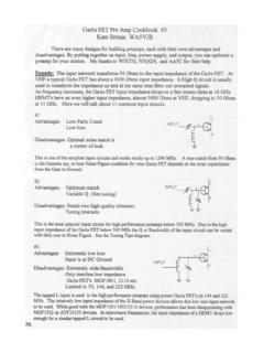
5 NGST s gaas ICs can be stored at 125 C indefinitely without damage. gaas chips are capable of surviving much higher temperatures for shorter times. Recommended Assembly ProcessFigure 1 shows a typical gaas IC chip Individual Chip Handling The metallization patterns on the frontside of the chip are very fragile. Any tool that contacts the frontside of the the chip, must be used with extreme caution. Vacuum pickup tools may be used on gaas chips, but NGST recommends that they be used only on the backside of the chip. It is recommended to use ESD composite tweezers. Note: Many of the NGST parts do incorporate airbridges, so caution should be used when determining the pick up tool. Personnel TrainingAssembly operators familiar only with silicon ICs, ceramic substrates, or even gaas FETs, should be retrained specifically for handling gaas chips.
6 NGST has learned that many people hired without previous gaas experience require a period of training and practice before they can safely and confidently handle gaas chips. Page 4 of 11 Note: The data contained in this document is for information only. northrop grumman reserves the right to change without notice the specifications, designs, prices or conditions of sale, as they apply to this product. The product represented by this datasheet is subject to Export Law as contained in ITAR or the EAR IC Application NoteMicroelectronic Products & Services Phone: (310) 814-5000 Fax: (310) 812-7011 E-mail: Web: : April 2008 Application Mounting ProcessesMost NGST gaas IC chips have a gold backing and can be mounted successfully using either a conductive epoxy or AuSn attachment.
7 NGST recommends the use of conductive epoxy due to the reduced mechanical strain placed on the chip. The two most important factors when mounting these MMICs are to provide a good thermal path and a good RF path to ground. This should be considered when determining the method for attachment. Possible Materials include:Eutectic AttachmentSilver EpoxyNote: Many of the NGST parts do incorporate airbridges, so caution should be used when determining the pick up tool. CAUTION: THE IMPROPER USE OF AuSn ATTACHMENT CAN CATASTROPHICALLY DAMAGE gaas CHIPS. THE DECISION TO USE AuSn ATTACHMENT AND THE RESPONSIBILITY FOR ANY RESULTING DAMAGE RESTS SOLELY WITH THE END INRF OUTVGVDGNDVd100 pF. 1 F100 FVg10 OhmsGroundingBondingRibbon / Wire BondResistorCapacitorsFigure 1. Representative gaas HEMT BondingPage 5 of 11 Note: The data contained in this document is for information only.
8 northrop grumman reserves the right to change without notice the specifications, designs, prices or conditions of sale, as they apply to this product. The product represented by this datasheet is subject to Export Law as contained in ITAR or the EAR IC Application NoteMicroelectronic Products & Services Phone: (310) 814-5000 Fax: (310) 812-7011 E-mail: Web: : April 2008 Application GroundingThe back of the chip is the ground plane so it is imperative that it sees a good ground connection. Without good grounding the chip could see an increased inductance and/or resistance to ground. The result of this is the potential for oscillations. It is recommended to mount the part straight to a thermally matched metal carrier (which will inherently provide a good path to ground).
9 Another option is to mount it onto a substrate, which itself is mounted to the carrier plate. If the chip is to be mounted to a substrate the grounding becomes critical. You need to insure that there are multiple ground vias, so as the top of the substrate now appears as a solid ground plane. Filled vias should always be used to help prevent resonance between grounds and to provide a good thermal interface. The Ground pads on the chip are for wafer probing only. They do not require being bonded. The On chip Ground pad SHOULD NOT be used as an alternative to providing the back plane with an adequate ground. Ribbon/Wire BondingNGST gaas IC chips have gold metallization on all bond/probe pads and are therefore suitable for both gold wire and ribbon bonding. When a proper bonding schedule is used, the bond strength and pad adhesion are capable of meeting the destructive bond pull limits in MIL_STD_883.
10 To attach the RFIN / RFOUT pads to the substrate either a ribbon or a wire can be used. The lengths should be kept to a minimum to limit the inductance and possible affect it can have on the performance of the chip. The preferred method is to use a wedge bond. The first Ribbon/Wire in the bias line (from the chip to the 100pF cap) is the most critical. If a long wire is used, it could form a series resonance with the 100pF cap and cause an 6 of 11 Note: The data contained in this document is for information only. northrop grumman reserves the right to change without notice the specifications, designs, prices or conditions of sale, as they apply to this product. The product represented by this datasheet is subject to Export Law as contained in ITAR or the EAR IC Application NoteMicroelectronic Products & Services Phone: (310) 814-5000 Fax: (310) 812-7011 E-mail: Web: : April 2008 Application Ribbon/Wire Bonding(cont.)