Transcription of Glass Passivated Single-Phase Bridge Rectifier
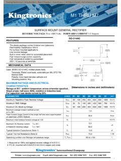
1 GBPC12, GBPC15, GBPC25, General Semiconductor Revision: 21-Feb-141 Document Number: 88612 For technical questions within your region: DOCUMENT IS SUBJECT TO CHANGE WITHOUT NOTICE. THE PRODUCTS DESCRIBED HEREIN AND THIS DOCUMENTARE SUBJECT TO SPECIFIC DISCLAIMERS, SET FORTH AT Passivated Single-Phase Bridge RectifierFEATURES UL recognition file number E54214 Universal 3-way terminals: snap-on, wire wrap-around, or PCB mounting Typical IR less than A High surge current capability Low thermal resistance Solder dip 275 C max. 10 s, per JESD 22-B106 Material categorization: For definitions of compliance please see TYPICAL APPLICATIONSG eneral purpose use in AC/DC Bridge full wave rectification for power supply, home appliances, office equipment, industrial automation DATACase: GBPC, GBPC-W Molding compound meets UL 94 V-0 flammability rating Base P/N-E4 - RoHS-compliant, commercial gradeTerminals: Nickel plated on faston lugs or silver plated on wire leads, solderable per J-STD-002 and JESD22-B102.
2 Suffix letter W added to indicate wire leads ( GBPC12005W).Polarity: As marked, positive lead by beveled cornerMounting Torque: 20 inches-lbs. CHARACTERISTICSP ackageGBPC, GBPC-WIF(AV)12 A, 15 A, 25 A, 35 AVRRM50 V to 1000 VIFSM200 A, 300 A, 300 A, 400 AIR5 AVF at VTJ CDiode variationsQuad~~~~GBPCGBPC-W~~MAXIMUM RATINGS (TA = 25 C unless otherwise noted)PARAMETERSYMBOLGBPC12, 15, 25, 35 UNIT005010204060810 Maximum repetitive peak reverse voltageVRRM501002004006008001000 VMaximum RMS voltage VRMS3570140280420560700 VMaximum DC blocking voltage VDC501002004006008001000 VMaximum average forward rectified output current (Fig. 1) GBPC12 IF (AV)12 AGBPC1515 GBPC2525 GBPC35 35 Peak forward surge current singlesine-wave superimposed on rated load GBPC12 IFSM200 AGBPC15300 GBPC25300 GBPC35 400 Rating (non-repetitive, for t greater than 1 ms and less than ms) for fusing GBPC12 I2t160 A2sGBPC15375 GBPC25375 GBPC35 660 RMS isolation voltage from case to leads VISO2500 VOperating junction storage temperature range TJ, TSTG - 55 to + 150 CGBPC12, GBPC15, GBPC25, General Semiconductor Revision: 21-Feb-142 Document Number.
3 88612 For technical questions within your region: DOCUMENT IS SUBJECT TO CHANGE WITHOUT NOTICE. THE PRODUCTS DESCRIBED HEREIN AND THIS DOCUMENTARE SUBJECT TO SPECIFIC DISCLAIMERS, SET FORTH AT (1)With heatsink(2)Bolt down on heatsink with silicone thermal compound between Bridge and mounting surface for maximum heat transfer with #10 screwELECTRICAL CHARACTERISTICS (TA = 25 C unless otherwise noted)PARAMETERTESTCONDITIONSSYMBOL GBPC12, 15, 25, 35 UNIT005 01 02 04 06 08 10 Maximum instantaneous forward drop per diodeGBPC12IF = = AGBPC25IF = AGBPC35 IF = AMaximum reverse DC current at ratedDC blocking voltage per diodeTA = 25 ATA = 125 C500 Typical junction capacitance per diode4 V, 1 MHzCJ300pFTHERMAL CHARACTERISTICS (TA = 25 C unless otherwise noted)PARAMETERSYMBOL GBPC12, 15, 25, 35 UNIT005 01 02 04 06 08 10 Typical thermal resistanceGBPC12 to GBPC25R JC (1)
4 C/WGBPC35 INFORMATION (Example)PREFERRED P/NUNIT WEIGHT (g)PREFERRED PACKAGE CODEBASE QUANTITYDELIVERY MODEGBPC1206-E4 boxGBPC1506-E4 boxGBPC2506-E4 boxGBPC3506-E4 boxGBPC1206W-E4 boxGBPC1506W-E4 boxGBPC2506W-E4 boxGBPC3506W-E4 boxGBPC12, GBPC15, GBPC25, General Semiconductor Revision: 21-Feb-143 Document Number: 88612 For technical questions within your region: DOCUMENT IS SUBJECT TO CHANGE WITHOUT NOTICE. THE PRODUCTS DESCRIBED HEREIN AND THIS DOCUMENTARE SUBJECT TO SPECIFIC DISCLAIMERS, SET FORTH AT AND CHARACTERISTICS CURVES (TA = 25 C unless otherwise noted) Fig. 1 - Maximum Output Rectified Current Fig. 2 - Maximum Output Rectified Current Fig. 3 - Maximum Power Dissipation Fig. 4 - Maximum Non-Repetitive Peak Forward SurgeCurrent Per Diode Fig. 5 - Typical Instantaneous Forward Characteristics Per Diode Fig. 6 - Typical Reverse Leakage Characteristics Per Diode02550751001251501752000520152510303 540 Bridges Mounted x x "( x x cm)AL, Finned Plate5 x 6 x "AL, Finned Plate5 x 4 x 3"AL, Finned Plate6 x x "AL, Finned Plate60 HzResistive orInductive LoadCase Temperature ( C)Average Forward Current (A)0 10 20 30 40 50 60 70 80 90 1000 5 10 15 20 25 30 35 40 60 HzResistive orInductive LoadGBPC35 RthSA = C/WGBPC15 RthSA = C/WGBPC12 RthSA = C/WGBPC25 RthSA = C/WAmbient Temperature ( C)Average Forward Current (A) Average Output Current (A)Average Power Dissipation of Bridge (W)01020304001020304050607080 Capacitive LoadTJ = TJ orInductive LoadNumber of Cycles at 60 HzPeak Forward Surge Current (A)110101000 GBPC35 GBPC15 GBPC25 GBPC12TJ = TJ ms Single CycleInstantaneous Forward Voltage (V)Instantaneous Forward Current (A) = 100 CTA = 150 CTA = 125 CTA = 25 of Rated Peak Reverse Voltage (%)Instantaneous Reverse LeakageCurrent ( A)
5 305070901000TA = 100 CTA = 150 CTA = 125 CTA = 25 C10 GBPC12, GBPC15, GBPC25, General Semiconductor Revision: 21-Feb-144 Document Number: 88612 For technical questions within your region: DOCUMENT IS SUBJECT TO CHANGE WITHOUT NOTICE. THE PRODUCTS DESCRIBED HEREIN AND THIS DOCUMENTARE SUBJECT TO SPECIFIC DISCLAIMERS, SET FORTH AT Fig. 7 - Typical Junction Capacitance Per Diode Fig. 8 - Typical Transient Thermal Impedance Per DiodePACKAGE OUTLINE DIMENSIONS in inches (millimeters)110100101001000TJ = 25 Cf = MHzVsig = 50 mVp-pReverse Voltage (V)Junction Capacitance (pF) = 25 Cf = MHzVsig = 50 mVp-pt - Heating Time (s)Transient Thermal Impedance ( C/W) ( ) ( ) ( ) ( ) ( ) ( ) ( ) ( ) ( ) ( ) ( ) ( ) ( ) ( ) ( )Hole for#10 ( ) ( ) ( ) ( ) ( ) ( ) ( ) ( ) ( ) ( ) ( ) ( ) ( ) ( ) ( ) ( ) ( ) ( ) ( ) ( ) ( ) ( ) ( ) ( ) ( ) ( ) ( ) ( ) ( ) ( )Hole for#10 ( ) ( ) Disclaimer Revision: 08-Feb-171 Document Number: 91000 Disclaimer ALL PRODUCT, PRODUCT SPECIFICATIONS AND DATA ARE SUBJECT TO CHANGE WITHOUT NOTICE TO IMPROVE RELIABILITY, FUNCTION OR DESIGN OR OTHERWISE.
6 vishay Intertechnology, Inc., its affiliates, agents, and employees, and all persons acting on its or their behalf (collectively, vishay ), disclaim any and all liability for any errors, inaccuracies or incompleteness contained in any datasheet or in any other disclosure relating to any makes no warranty, representation or guarantee regarding the suitability of the products for any particular purpose or the continuing production of any product. To the maximum extent permitted by applicable law, vishay disclaims (i) any and all liability arising out of the application or use of any product, (ii) any and all liability, including without limitation special, consequential or incidental damages, and (iii) any and all implied warranties, including warranties of fitness for particular purpose, non-infringement and merchantability. Statements regarding the suitability of products for certain types of applications are based on vishay s knowledge of typical requirements that are often placed on vishay products in generic applications.
7 Such statements are not binding statements about the suitability of products for a particular application. It is the customer s responsibility to validate that a particular product with the properties described in the product specification is suitable for use in a particular application. Parameters provided in datasheets and / or specifications may vary in different applications and performance may vary over time. All operating parameters, including typical parameters, must be validated for each customer application by the customer s technical experts. Product specifications do not expand or otherwise modify vishay s terms and conditions of purchase, including but not limited to the warranty expressed as expressly indicated in writing, vishay products are not designed for use in medical, life-saving, or life-sustaining applications or for any other application in which the failure of the vishay product could result in personal injury or death.
8 Customers using or selling vishay products not expressly indicated for use in such applications do so at their own risk. Please contact authorized vishay personnel to obtain written terms and conditions regarding products designed for such license, express or implied, by estoppel or otherwise, to any intellectual property rights is granted by this document or by any conduct of vishay . Product names and markings noted herein may be trademarks of their respective owners. 2017 vishay INTERTECHNOLOGY, INC. ALL RIGHTS RESERVED