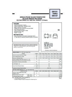
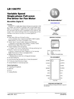
Transcription of Glass Passivated Single-Phase Bridge Rectifier
1 GBU4A, GBU4B, GBU4D, GBU4G, GBU4J, GBU4K, General Semiconductor Revision: 05-Aug-151 Document Number: 88614 For technical questions within your region: DOCUMENT IS SUBJECT TO CHANGE WITHOUT NOTICE. THE PRODUCTS DESCRIBED HEREIN AND THIS DOCUMENTARE SUBJECT TO SPECIFIC DISCLAIMERS, SET FORTH AT Passivated Single-Phase Bridge RectifierFEATURES UL recognition file number E54214 Ideal for printed circuit boards High surge current capability High case dielectric strength of 1500 VRMS Solder dip 275 C max. 10 s, per JESD 22-B106 Material categorization: for definitions of compliance please see TYPICAL APPLICATIONSG eneral purpose use in AC/DC Bridge full wave rectification for monitor, TV, printer, switching mode power supply, adapter, audio equipment, and home appliances DATACase: GBU Molding compound meets UL 94 V-0 flammability rating Base P/N-E3 - RoHS-compliant, commercial gradeTerminals: Matte tin plated leads, solderable per J-STD-002 and JESD 22-B102 E3 suffix meets JESD 201 class 1A whisker testPolarity: As marked on bodyMounting Torque: 10 cm-kg ( inches-lbs) Torque.
2 Cm-kg (5 inches-lbs)Notes(1)Unit case mounted on " x " x " thick ( cm x cm x cm) aluminum plate(2)Units mounted on PCB with " x " (12 mm x 12 mm) copper pads and " ( mm) lead lengthPRIMARY CHARACTERISTICSP ackageGBUIF(AV) AVRRM50 V, 100 V, 200 V, 400 V, 600 V, 800 V, 1000 VIFSM150 AIR5 AVF at IF = VTJ CDiode variationsIn-lineCase Style GBU- ~ ~ +Case Style GBU+~~-~~MAXIMUM RATINGS (TA = 25 C unless otherwise noted)PARAMETER SYMBOL GBU4A GBU4B GBU4D GBU4G GBU4J GBU4K GBU4M UNIT Maximum repetitive peak reverse voltage VRRM 50 100 200 400 600 800 1000 V Maximum RMS voltage VRMS 35 70 140 280 420 560 700 V Maximum DC blocking voltage VDC 50 100 200 400 600 800 1000 V Maximum average forward rectified output current at TC = 100 C (1)IF(AV) TA = 40 C (2) forward surge current single sine-wave superimposed on rated loadIFSM 150A Rating for fusing (t < ms)
3 I2t 93A2s Operating junction and storage temperature range TJ, TSTG -55 to +150 C GBU4A, GBU4B, GBU4D, GBU4G, GBU4J, GBU4K, General Semiconductor Revision: 05-Aug-152 Document Number: 88614 For technical questions within your region: DOCUMENT IS SUBJECT TO CHANGE WITHOUT NOTICE. THE PRODUCTS DESCRIBED HEREIN AND THIS DOCUMENTARE SUBJECT TO SPECIFIC DISCLAIMERS, SET FORTH AT (1)Units case mounted on aIuminum plate heatsink(2)Units mounted in free air, no heatsink on PCB, " x " (12 mm x 12 mm) copper pads, " ( mm) lead lengthRATINGS AND CHARACTERISTICS CURVES (TA = 25 C unless otherwise noted) Fig. 1 - Derating Curve Output Rectified CurrentFig.
4 2 - Maximum Non-Repetitive Peak Forward SurgeCurrent Per DiodeELECTRICAL CHARACTERISTICS (TA = 25 C unless otherwise noted)PARAMETER TEST CONDITIONS SYMBOL GBU4A GBU4B GBU4D GBU4G GBU4J GBU4K GBU4M UNIT Maximum instantaneous forward voltage drop per diode A VF Maximum DC reverse current at rated DC blocking voltage per diodeTA = 25 CIR A TA = 125 C500 Typical junction capacitance per diode 4 V, 1 MHz CJ 57pFTHERMAL CHARACTERISTICS (TA = 25 C unless otherwise noted)PARAMETERSYMBOL GBU4A GBU4B GBU4D GBU4G GBU4J GBU4K GBU4M UNITT ypical thermal resistanceR JA (2)22 C/WR JC (1) INFORMATIONPREFERRED P/NUNIT WEIGHT (g)PREFERRED PACKAGE CODEBASE QUANTITYDELIVERY MODEGBU4J-E3 ( C)Average Forward Output Current (A)Heatsink Mounting, x x " Thickness( x x cm) Al.
5 Mounting, x " (12 x 12 mm) Copper " ( mm) Lead Length60 Hz Resistive or Inductive Load CycleTJ = TJ Sine-WaveNumber of Cycles at 60 HzPeak Forward Surge Current (A)GBU4A, GBU4B, GBU4D, GBU4G, GBU4J, GBU4K, General Semiconductor Revision: 05-Aug-153 Document Number: 88614 For technical questions within your region: DOCUMENT IS SUBJECT TO CHANGE WITHOUT NOTICE. THE PRODUCTS DESCRIBED HEREIN AND THIS DOCUMENTARE SUBJECT TO SPECIFIC DISCLAIMERS, SET FORTH AT 3 - Typical Forward Characteristics Per DiodeFig. 4 - Typical Reverse Leakage Characteristics Per DiodeFig. 5 - Typical Junction Capacitance Per DiodeFig. 6 - Typical Transient Thermal ImpedancePACKAGE OUTLINE DIMENSIONS in inches (millimeters) Forward Voltage (V)Instantaneous Forward Current (A)TJ = 25 CPulse Width = 300 s1 % Duty Reverse Current ( A)Percent of Rated Peak Reverse Voltage (%)TA= 150 CTA= 125 CTA= 100 CTA= 25 Capacitance (pF)Reverse Voltage (V)TJ= 25 Cf = MHzVsig= 50 - Heating Time (s)Transient Thermal Impedance ( C/W)Case Type GBUP olarity shown on front side of case, positive lead by beveled ( ) x 45 ( ) ( ) R (TYP.)
6 ( ) ( ) ( ) ( ) ( ) ( ) ( ) ( ) ( ) ( ) ( ) ( ) ( ) ( ) ( )9 ( ) ( ) ( ) ( ) ( ) ( ) ( ) ( ) ( ) ( ) ( ) ( )Legal Disclaimer Revision: 08-Feb-171 Document Number: 91000 Disclaimer ALL PRODUCT, PRODUCT SPECIFICATIONS AND DATA ARE SUBJECT TO CHANGE WITHOUT NOTICE TO IMPROVE RELIABILITY, FUNCTION OR DESIGN OR OTHERWISE. vishay Intertechnology, Inc., its affiliates, agents, and employees, and all persons acting on its or their behalf (collectively, vishay ), disclaim any and all liability for any errors, inaccuracies or incompleteness contained in any datasheet or in any other disclosure relating to any makes no warranty, representation or guarantee regarding the suitability of the products for any particular purpose or the continuing production of any product.
7 To the maximum extent permitted by applicable law, vishay disclaims (i) any and all liability arising out of the application or use of any product, (ii) any and all liability, including without limitation special, consequential or incidental damages, and (iii) any and all implied warranties, including warranties of fitness for particular purpose, non-infringement and merchantability. Statements regarding the suitability of products for certain types of applications are based on vishay s knowledge of typical requirements that are often placed on vishay products in generic applications. Such statements are not binding statements about the suitability of products for a particular application.
8 It is the customer s responsibility to validate that a particular product with the properties described in the product specification is suitable for use in a particular application. Parameters provided in datasheets and / or specifications may vary in different applications and performance may vary over time. All operating parameters, including typical parameters, must be validated for each customer application by the customer s technical experts. Product specifications do not expand or otherwise modify vishay s terms and conditions of purchase, including but not limited to the warranty expressed as expressly indicated in writing, vishay products are not designed for use in medical, life-saving, or life-sustaining applications or for any other application in which the failure of the vishay product could result in personal injury or death.
9 Customers using or selling vishay products not expressly indicated for use in such applications do so at their own risk. Please contact authorized vishay personnel to obtain written terms and conditions regarding products designed for such license, express or implied, by estoppel or otherwise, to any intellectual property rights is granted by this document or by any conduct of vishay . Product names and markings noted herein may be trademarks of their respective owners. 2017 vishay INTERTECHNOLOGY, INC. ALL RIGHTS RESERVED