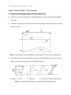
Transcription of How to Read a Datasheet - Michigan State University
1 How to Read a Datasheet Prepared for the WIMS outreach program 5/6/02, D. Grover In order to use a PIC microcontroller, a flip-flop, a photodetector, or practically any electronic device, you need to consult a Datasheet . This is the document that the manufacturer provides telling you the typical device performance minimum and maximum requirements and characteristics what you can do to the device without harming it suggested uses and hints Manufacturers want you, the designer, to have a successful experience with their device. They are trying to be helpful. They don t always succeed. The Datasheet on the following pages is a relatively good Datasheet . It tries to concisely tell you everything you need to know about the device, a common 555 timer chip (the duct-tape of the electronics hobbyist).
2 Most datasheets for ICs follow the same general layout. You don t have to understand everything in a Datasheet . There s a lot of information that might not be of any use to you. The annotations that follow try to point out parts of the Datasheet that you should pay particular attention to. Where do you find datasheets? Nowadays you can find almost any Datasheet on the internet, often in PDF (Acrobat) form. For example, the LM555 Datasheet from National Semiconductor is on their website at What is the LM555? The LM555 is a timer chip that uses external resistors and capacitors to generate either a single pulse of a certain duration, or a continuous sequence of pulses with a variety of pulse widths possible.
3 Because it is a very general purpose collection of functional blocks such as comparators , a flip-flop, internal voltage divider, high power output stage, and so on, a number of different timing-related functions are possible. Entire books have been written about the 555, though it is often used when another IC would work better. (See for example the CD4538 timer chip.) LM555 TimerGeneral DescriptionThe LM555 is a highly stable device for generating accuratetime delays or oscillation. Additional terminals are providedfor triggering or resetting if desired. In the time delay mode ofoperation, the time is precisely controlled by one external re-sistor and capacitor. For astable operation as an oscillator,the free running frequency and duty cycle are accuratelycontrolled with two external resistors and one capacitor.
4 Thecircuit may be triggered and reset on falling waveforms, andthe output circuit can source or sink up to 200mA or driveTTL replacement for SE555/NE555nTiming from microseconds through hoursnOperates in both astable and monostable modesnAdjustable duty cyclenOutput can source or sink 200 mAnOutput and supply TTL compatiblenTemperature stability better than per CnNormally on and normally off outputnAvailable in 8-pin MSOP packageApplicationsnPrecision timingnPulse generationnSequential timingnTime delay generationnPulse width modulationnPulse position modulationnLinear ramp generatorSchematic DiagramDS007851-1 February 2000LM555 Timer 2000 National Semiconductor DiagramOrdering InformationPackagePart NumberPackage MarkingMedia TransportNSC Drawing8-Pin
5 Units Tape and Reel8-Pin MSOPLM555 CMMZ551k Units Tape and Units Tape and Reel8-Pin MDIPLM555 CNLM555 CNRailsN08 EDual-In-Line, Small Outlineand Molded Mini Small Outline PackagesDS007851-3 Top Maximum Ratings(Note 2)If Military/Aerospace specified devices are required,please contact the National Semiconductor Sales Office/Distributors for availability and Voltage+18 VPower Dissipation (Note 3)LM555CM, LM555CN1180 mWLM555 CMM613 mWOperating Temperature RangesLM555C0 C to +70 CStorage Temperature Range 65 C to +150 CSoldering InformationDual-In-Line PackageSoldering (10 Seconds)260 CSmall Outline Packages(SOIC and MSOP)Vapor Phase (60 Seconds)215 CInfrared (15 Seconds)220 CSee AN-450 Surface Mounting Methods and Their Effecton Product Reliability for other methods of solderingsurface mount Characteristics(Notes 1, 2)(TA= 25 C, VCC= +5V to +15V, unless othewise specified)ParameterConditionsLimitsUnits LM555 CMinTypMaxSupply CurrentVCC= 5V, RL= VCC= 15V, RL= (Low State ) (Note 4)310615mATiming Error, MonostableInitial Accuracy1%Drift with TemperatureRA= 1k to 100k ,50ppm/ CC = F, (Note 5)Accuracy over with Error, AstableInitial with TemperatureRA,RB= 1k to 100k ,150ppm/ CC = F, (Note 5)Accuracy over with VCCT rigger VoltageVCC= 15V5 VVCC= AReset Current(Note 6)
6 AControl Voltage LevelVCC= 15 VVCC= 7 Leakage Output High1100nAPin 7 Sat (Note 7)Output LowVCC= 15V, I7= 15mA180mVOutput LowVCC= , I7= Characteristics(Notes 1, 2) (Continued)(TA= 25 C, VCC= +5V to +15V, unless othewise specified)ParameterConditionsLimitsUnits LM555 CMinTypMaxOutput Voltage Drop (Low)VCC= 15 VISINK= 8mAVISINK= Voltage Drop (High)ISOURCE= 200mA, VCC= 100mA, VCC= Time of Output100nsFall Time of Output100nsNote 1:All voltages are measured with respect to the ground pin, unless otherwise 2:Absolute Maximum Ratings indicate limits beyond which damage to the device may occur. Operating Ratings indicate conditions for which the device is func-tional, but do not guarantee specific performance limits.
7 Electrical Characteristics State DC and AC electrical specifications under particular test conditions which guar-antee specific performance limits. This assumes that the device is within the Operating Ratings. Specifications are not guaranteed for parameters where no limit isgiven, however, the typical value is a good indication of device 3:For operating at elevated temperatures the device must be derated above 25 C based on a +150 C maximum junction temperature and a thermal resistanceof 106 C/W (DIP), 170 C/W (S0-8), and 204 C/W (MSOP) junction to 4:Supply current when output high typically 1 mA less at VCC= 5:Tested at VCC= 5V and VCC= 6:This will determine the maximum value of RA+RBfor 15V operation.
8 The maximum total (RA+RB)is20M .Note 7:No protection against excessive pin 7 current is necessary providing the package dissipation rating will not be 8:Refer to RETS555X drawing of military LM555H and LM555J versions for Performance CharacteristicsMinimuim Pulse WidthRequired for TriggeringDS007851-4 Supply Current VoltageDS007851-19 High Output Voltage Source CurrentDS007851-20 Low Output Voltage Sink CurrentDS007851-21 Low Output Voltage Sink CurrentDS007851-22 Low Output Voltage Sink InformationMONOSTABLE OPERATIONIn this mode of operation, the timer functions as a one-shot(Figure 1). The external capacitor is initially held dischargedby a transistor inside the timer. Upon application of a nega-tive trigger pulse of less than 1/3 VCCto pin 2, the flip-flop isset which both releases the short circuit across the capacitorand drives the output voltage across the capacitor then increases exponen-tially for a period of t = RAC, at the end of which time thevoltage equals 2/3 VCC.
9 The comparator then resets theflip-flop which in turn discharges the capacitor and drives theoutput to its low 2shows the waveforms gener-ated in this mode of operation. Since the charge and thethreshold level of the comparator are both directly propor-tional to supply voltage, the timing internal is independent the timing cycle when the output is high, the furtherapplication of a trigger pulse will not effect the circuit so longas the trigger input is returned high at least 10 s before theend of the timing interval. However the circuit can be resetduring this time by the application of a negative pulse to thereset terminal (pin 4). The output will then remain in the lowstate until a trigger pulse is again the reset function is not in use, it is recommended thatit be connected to VCCto avoid any possibility of false 3is a nomograph for easy determination of R, C val-ues for various time :In monostable operation, the trigger should be drivenhigh before the end of timing OPERATIONIf the circuit is connected as shown inFigure 4(pins 2 and 6connected) it will trigger itself and free run as a external capacitor charges through RA+RBand dis-charges through RB.
10 Thus the duty cycle may be preciselyset by the ratio of these two this mode of operation, the capacitor charges and dis-charges between 1/3 VCCand 2/3 VCC. As in the triggeredmode, the charge and discharge times, and therefore the fre-quency are independent of the supply 1. MonostableDS007851-6 VCC= 5 VTop Trace: Input 5 = Trace: Output 5 Bottom Trace: Capacitor Voltage 2 = FFIGURE 2. Monostable WaveformsDS007851-7 FIGURE 3. Time DelayDS007851-8 FIGURE 4. Dimensionsinches (millimeters) unless otherwise noted (Continued)LIFE SUPPORT POLICYNATIONAL S PRODUCTS ARE NOT AUTHORIZED FOR USE AS CRITICAL COMPONENTS IN LIFE SUPPORTDEVICES OR SYSTEMS WITHOUT THE EXPRESS WRITTEN APPROVAL OF THE PRESIDENT AND GENERALCOUNSEL OF NATIONAL SEMICONDUCTOR CORPORATION.